Discover our highly specialized, application-specific printed circuit board assemblies engineered for safety-critical, medical, automotive, and industrial domains.
Bridging engineering complexity with scalable execution to deliver market-leading commercial results.
Strict adherence to IATF 16949 guidelines, delivering thermal shock resistance, zero-defect production pathways, and double-sided PCBA designs tailored for On-board Chargers (OBC), ADAS systems, and EV Powertrains.
ISO 13485 certified micro-electronic assemblies designed for life-support devices, diagnostic monitors, and wearable patient telemetry systems. Full traceability on every component down to batch codes.
Heavy copper PCB construction, specialized potting, and conformal coating solutions designed to withstand extreme thermal ranges, vibrations, and high voltages in demanding grid infrastructure environments.
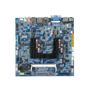
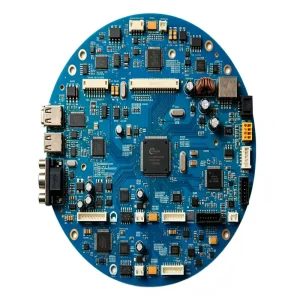
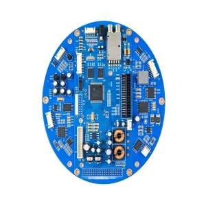
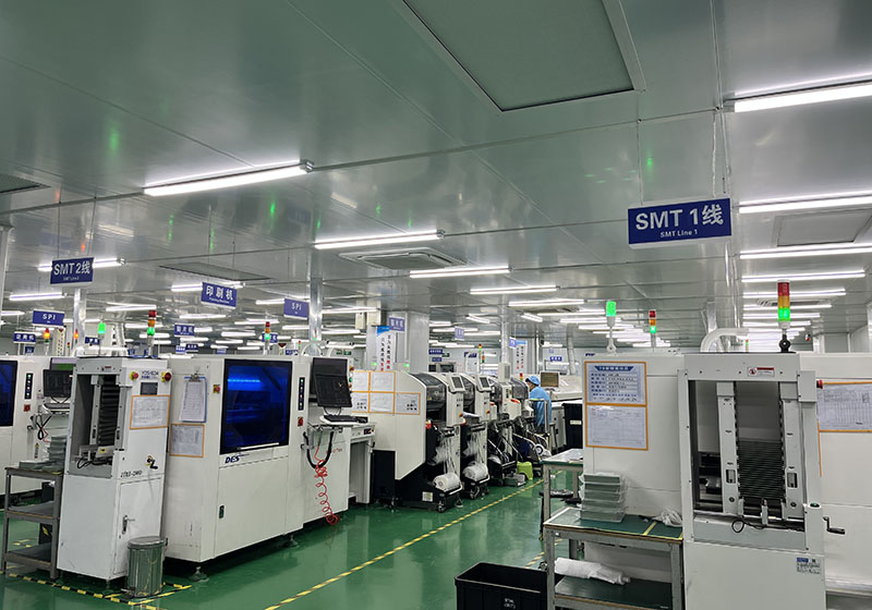
In modern industrial applications, seeking high-quality OEM make PCB manufacturers is no longer just about buying raw boards; it is a critical optimization of the product life cycle. From the design of complex high-density interconnect (HDI) layers to the structural constraints of automated optical inspections (AOI), quality and precision govern market execution. Shenzhen STHL, founded in 2006, operates at the center of this paradigm, bridging high-mix low-volume (HMLV) agility with high-volume production capabilities across a massive 10,000 sqm footprint.
By leveraging certified quality systems including IATF 16949 for critical automotive modules and ISO 13485 for medical-grade apparatus, STHL enforces a comprehensive Zero-Defect framework. Our engineering methodologies inspect, source, and assemble boards from double-sided surface mount topologies up to complex rigid-flex multilayer assemblies, providing a global client network across 90+ countries with unmatched manufacturing security.
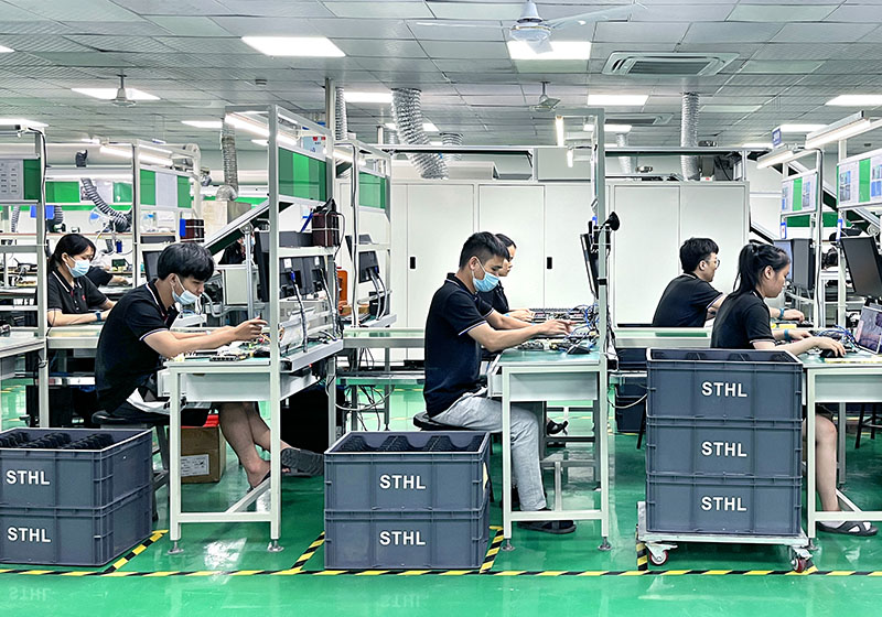
Shenzhen STHL is a premier partner for turn-key electronics manufacturing services (EMS) in China. We support global clients across the entire product lifecycle—from schematic optimization and DFM (Design for Manufacturability) analysis, component procurement, to high-precision PCB fabrication, SMT assembly, manual THT integration, box-build integration, and definitive functional testing.
Our infrastructure is optimized to minimize overhead and protect production schedules: our 10,000 sqm advanced facility employs over 220 skilled workers and features 7 fully-automated SMT placement lines, 2 DIP/THT lines, 2 dedicated functional testing (FCT) setups, and 2 end-to-end device assembly/box-build lines. This capacity ensures smooth scaling from dynamic prototypes to high-speed mass production runs.
Our international presence spans the USA, Germany, Italy, UK, Poland, New Zealand, Argentina, Brazil, Turkey, Korea, Thailand, and over 90 regions globally. This wide exposure has allowed STHL to align our quality assurance frameworks directly with the demanding standards of western markets, producing electronics that comply fully with RoHS and REACH mandates.
Precision placement is critical for modern component geometries. Our SMT operations deploy high-speed Pick-and-Place machinery designed to process components down to 01005 passives and ultra-fine pitch micro-BGAs (<0.4mm pitch) with micro-level alignment tolerances.
Our technicians handle a comprehensive range of advanced chip geometries: Ball Grid Arrays (BGA), Micro-BGAs (uBGA), QFN, QFP, SOIC, PLCC packaging formats, as well as complex stack-ups like Package-on-Package (PoP) assemblies. This capacity allows us to fit high-density processing power into tight, modern product profiles.
Quality control is integrated at every stage. We utilize automated solder paste inspection (SPI), multi-angle 3D Automated Optical Inspection (AOI), and high-resolution 3D X-Ray transmission radiography to inspect hidden solder joints under BGAs. This allows us to ensure void-free contact surfaces and eliminate defects like bridges, head-in-pillow joints, and micro-cracks before products leave the factory floor.
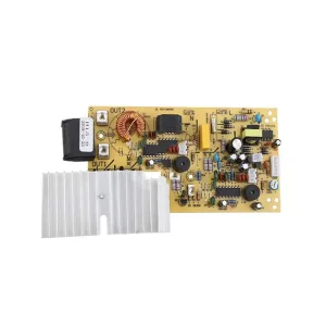
For applications subjected to persistent mechanical strain or high current density, Through-Hole Technology (THT) remains essential. STHL supports full-range THT processing, including selective wave soldering and custom fixture-guided wave soldering lines.
Our dual approach combines automatic high-speed insertion machinery for standardized components with specialized hand-soldering stations for complex parts. This setup is managed using custom ESD-safe and anti-static fixtures, ensuring uniform thermal exposure across complex multi-layer boards during wave passage.
Our manufacturing processes adhere to strict environmental standards. Our wave soldering machines are set up to process lead-free solder alloys in compliance with international RoHS requirements. Completed assemblies then undergo visual inspection (microscopic verification) and functional testing to confirm joint integrity and electrical safety.
A single source from raw design files to tested, packaged, and market-ready products.
We run 7 automated assembly lines handling both prototypes and bulk manufacturing. Our SMT setup delivers precise alignment, while our THT capabilities offer robust mechanical connections using RoHS-compliant lead-free processes.
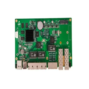
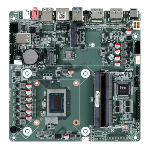
We manufacture high-reliability PCBs ranging from basic single-sided and double-sided layouts to multi-layered, flexible, and rigid-flex designs. Our production runs use premium laminates and precise plating to ensure reliable impedance performance.
Leveraging direct relationships with certified global component manufacturers and franchised distributors, we source genuine parts, manage lead times, and perform component verification inspections to keep production on schedule.
Our custom cable and wire harness manufacturing processes deliver high-durability shielding, precision overmolding, robust retention systems, and reliable connectors suited for automotive, industrial, and high-frequency communication projects.
We provide full system integration, from mounting PCB assemblies into custom custom enclosures to installing wire looms, front panel components, power supplies, and performing full final functional testing.
We design custom functional test setups that replicate actual operating conditions to verify electrical, signal, and power paths. This rigorous process prevents component damage and ensures reliable product performance prior to shipment.
The global electronics market faces continuous challenges, including material shortages and changing trade requirements. To maintain production stability, OEM partners need dynamic, resilient sourcing structures rather than simple supply lists.
STHL manages these dynamics through direct integration with key component networks. This setup allows us to source verified, traceably certified components, reducing the risk of counterfeit parts while finding alternative replacements during supply constraints to keep lines running.
Furthermore, our compliance with standards like IATF 16949, ISO 13485, and RoHS/REACH ensures that all assemblies satisfy the regulatory requirements of different regions, including North America, Europe, and the APAC market. This simplifies the import and certification processes for our global customers.
We evaluate trace tolerances, layout spacing, pad geometry, and thermal footprints prior to production to prevent assembly issues and improve production yields.
Our ERP tracking records production batches down to specific component reels. This provides reliable diagnostics and accountability for medical and automotive industries.
We test boards under simulated stress conditions, verifying resistance to humidity, thermal shifts, and current loads to ensure long-term field stability.
Aligning with the next generation of power electronics, high-speed networking, and computing architectures.
Integrating ceramic fillers, high-Tg FR-4, Rogers laminates, and heavy copper planes to manage the thermal loads and high frequencies of modern silicon carbide (SiC) and gallium nitride (GaN) power systems.
Developing laser-drilled microvias, stacked configurations, and ultra-fine trace routing (down to 2mil line/space). This supports dense component packages and reduces layers in space-constrained wearables and computing modules.
Deploying smart SPI-to-SMT feedback loops and machine-learning-enhanced optical inspection systems to optimize solder paste placement and target zero defects in large-scale assembly runs.
Key technical answers to common questions about layout, manufacturing capability, quality control, and supply chain management.
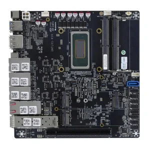
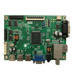
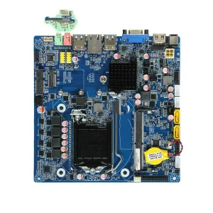
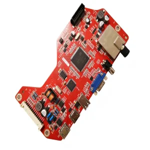
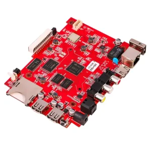
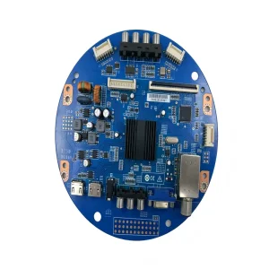
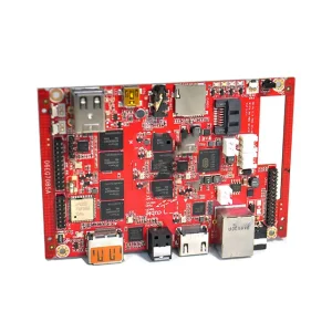
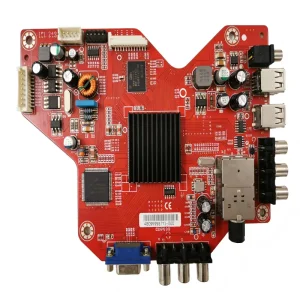
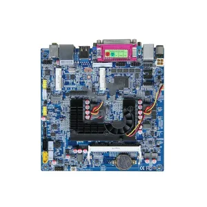
Further precision assemblies manufactured for display technology, audio processing, and commercial hardware environments.