Engineered to meet the rigorous performance, thermal, and mechanical standards of Bay Area hardware developers.
Heavy-duty control boards optimized for industrial robotics and automated manufacturing lines in the Bay Area.
View Details →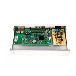
High-definition imaging and AI-edge processing integration for next-gen physical security systems.
View Details →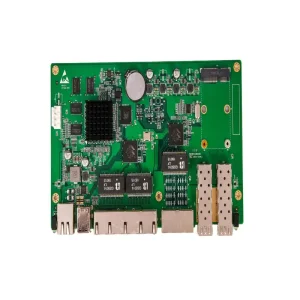
Multi-channel video recording boards featuring low-latency data bus routing and high thermal dissipation.
View Details →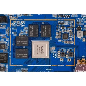
Ultra-thin, multi-layer HDI boards designed for high-performance computing and enterprise mobile devices.
View Details →How local innovation drives the need for high-density, reliable, and rapid-scaling electronics manufacturing.
San Francisco and the broader Silicon Valley region remain the global epicenter of hardware innovation. From autonomous vehicle systems in the Mission District to medical robotics in South San Francisco, and IoT smart-home startups in SoMa, the demand for cutting-edge Printed Circuit Board Assembly (PCBA) has shifted. It is no longer just about basic assembly; it is about managing extreme component density, high-frequency signals, and stringent thermal profiles.
Startups and established enterprises in San Francisco require a manufacturing partner that understands this dynamic. While local prototyping is essential for initial proof-of-concept, scaling to commercial production requires a seamless bridge to high-capacity, certified factories. STHL serves as this critical link, providing San Francisco businesses with the engineering depth of a local partner and the cost, speed, and supply chain resilience of our state-of-the-art Shenzhen facility.
Our services are tailored to support the unique lifecycle of Bay Area tech companies: rapid Design for Manufacturability (DFM) feedback during the R&D phase, followed by NPI (New Product Introduction) protocols, and finally, seamless transition to mass production with full traceability and compliance.
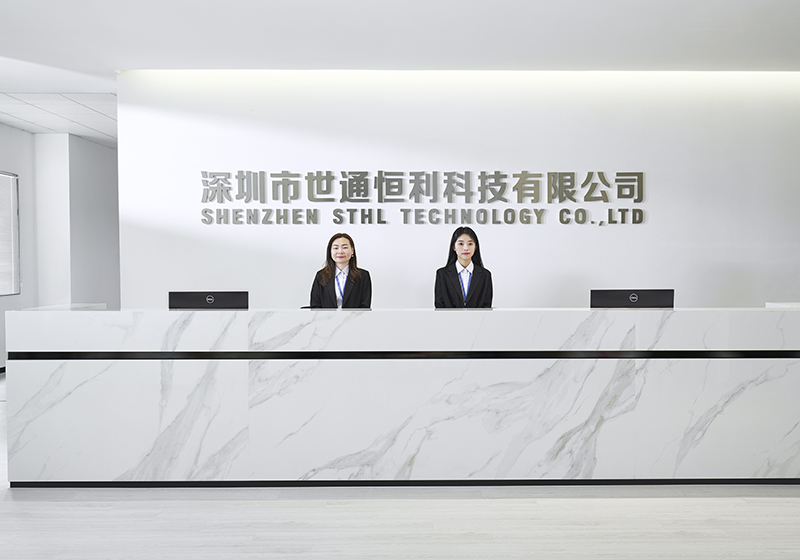
Shenzhen STHL is a premier provider of electronics manufacturing services (EMS) in China, serving customers worldwide along the entire industry chain. Our capabilities encompass PCB layout, component sourcing, PCB fabrication, PCBA assembly, cable assembly, box build assembly, and comprehensive testing services.
Established in 2006, STHL brings nearly two decades of contract electronics manufacturing experience to the table. Our 10,000 sqm facility houses over 220 skilled staff members, operating 7 SMT assembly lines, 2 DIP/THT lines, 2 functional testing lines, and 2 finished device assembly lines.
We cater to diverse sectors including energy power, communications, automotive, medical, consumer electronics, storage, and safety & security. Our client base spans the USA, Germany, Italy, UK, Poland, New Zealand, Brazil, and beyond. As an IATF16949, ISO9001, ISO14001, and ISO13485 certified manufacturer, we guarantee strict compliance with RoHS standards and rigorous quality assurance protocols.
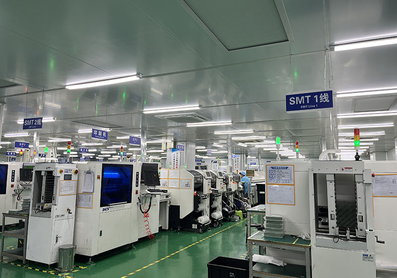
Surface Mount Technology (SMT) is the backbone of modern electronics. At STHL, we have refined our processes to handle the most complex and miniature components required by today's high-tech applications.
Our commitment to quality is backed by advanced inspection methodologies, including 3D SPI (Solder Paste Inspection), 3D AOI (Automated Optical Inspection), and high-resolution X-Ray analysis for hidden solder joints.
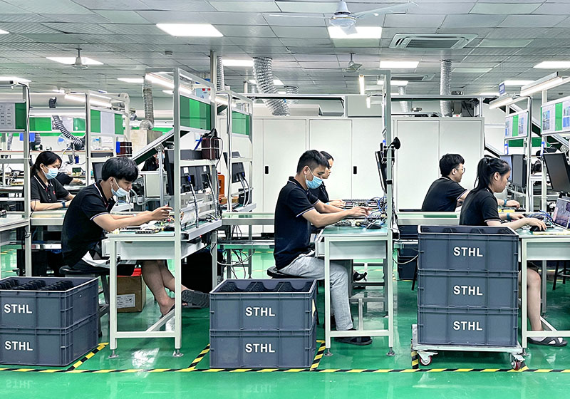
For power electronics, connectors, and components subjected to high mechanical stress, Through-Hole Technology remains irreplaceable. STHL offers robust THT solutions to complement our SMT lines.
Every THT assembly undergoes rigorous visual inspection and functional testing (FCT) to ensure electrical continuity and mechanical strength under harsh operating conditions.
From initial PCB fabrication to complete box-build assembly and functional testing.
Operating 7 automated SMT lines and 2 THT lines. We handle prototype runs to high-volume production with precise component placement and RoHS-compliant lead-free soldering.
Manufacturing high-quality, multi-layer rigid, flexible, and rigid-flex printed circuit boards. We utilize premium base laminates to meet tight impedance tolerances and mechanical specs.
Global supply chain network ensuring access to genuine, traceable components. We mitigate risks of counterfeits, allocation shortages, and long lead times to protect your timeline.
Precision manufacturing of wire harnesses and cable assemblies. Includes custom connectors, shielding, and strain relief systems engineered for harsh industrial environments.
Full system integration services. We mount PCBAs into custom enclosures, route internal cabling, install user interfaces, and deliver fully packaged, shelf-ready products.
Comprehensive electrical testing, firmware flashing, and environmental stress screening. We ensure 100% functional compliance before products leave our facility.
How our technical capabilities align with the specific requirements of San Francisco's leading sectors.
South San Francisco's biotech hub requires ultra-reliable, ISO 13485-compliant PCBAs for diagnostic tools, wearable patient monitors, and surgical robotics. We implement strict lot traceability, cleanroom assembly options, and rigorous testing to guarantee patient safety and device efficacy.
With automotive tech companies headquartered throughout the Bay Area, we provide IATF 16949-certified manufacturing. Our boards handle high-current power distribution, sensor fusion processing (LiDAR/Radar), and extreme thermal cycling common in electric vehicle platforms.
San Francisco's smart home and industrial IoT startups require compact, low-power PCBAs. We specialize in fine-pitch SMT, rigid-flex substrates for tight enclosures, and integrated RF testing (Wi-Fi, Bluetooth, LoRa, 5G) to ensure seamless wireless connectivity.
Why pairing San Francisco design with Shenzhen manufacturing yields the ultimate competitive edge.
Shenzhen is home to the world's most concentrated electronics supply chain. This proximity allows STHL to source raw materials, specialized substrates, and rare components in a fraction of the time it takes elsewhere. If a component goes on allocation, our localized procurement team can quickly identify drop-in replacements or source from authorized regional distributors.
We bridge the gap between low-volume quick-turn prototyping and high-volume mass production. Our engineering team performs comprehensive DFM (Design for Manufacturability) reviews on your Gerber files to catch potential assembly issues before fabrication begins, saving weeks of troubleshooting and costly board spins.
We understand that intellectual property is the lifeblood of San Francisco technology firms. STHL employs strict data security protocols, non-disclosure agreements (NDAs), and segmented network access to ensure your design files, firmware, and proprietary schematics remain completely secure throughout the manufacturing process.
Automotive-grade quality management systems for safety-critical applications.
Medical device manufacturing standards ensuring traceablity and cleanliness.
Global standards for quality management and environmental responsibility.
Strict adherence to international acceptability standards for electronic assemblies.
Preparing your hardware designs for the next generation of electronics manufacturing.
As chips shrink and pin counts rise, HDI technology utilizing microvias, blind/buried vias, and build-up layers becomes critical. Our roadmap includes expanding laser-drilling capabilities to support sub-0.1mm microvias for ultra-compact IoT and wearable applications.
Placing passive and active components directly inside the PCB substrate layer to save surface space, improve signal integrity, and enhance thermal performance. This is particularly beneficial for high-frequency RF and radar applications.
Integrating machine learning algorithms into our 3D AOI and X-ray systems to predict and prevent defects in real-time. By analyzing solder paste deposition patterns, we can adjust stencil alignment dynamically, driving defect rates closer to zero.
Technical insights and logistics answers for San Francisco hardware developers.
High-precision manufacturing services optimized for global distribution and local integration.
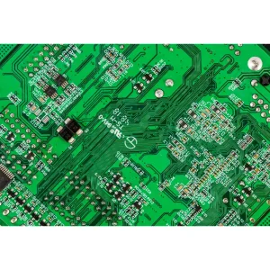
Multi-band RF routing and impedance-controlled board layouts for enterprise networking hardware.
View Details →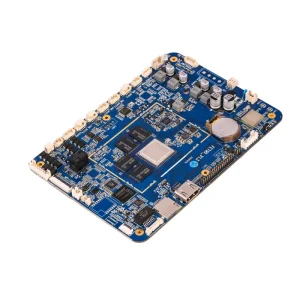
Reliable multi-layer boards featuring high thermal dissipation for continuous outdoor security operations.
View Details →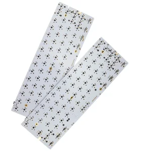
Metal-core PCBs (MCPCB) designed for optimal thermal management in high-brightness commercial fixtures.
View Details →
IPC Class 3 compliant assemblies built to withstand extreme vibration, thermal shock, and vacuum conditions.
View Details →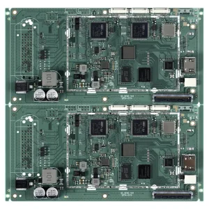
Compact, power-efficient circuit boards designed for smart thermostats, locks, and home automation hubs.
View Details →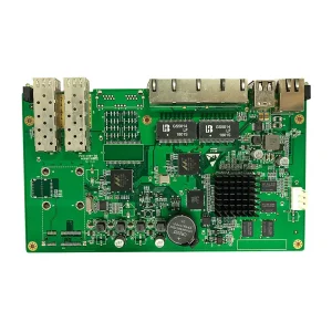
Fail-safe circuit designs for access control panels, fire alarms, and emergency communication networks.
View Details →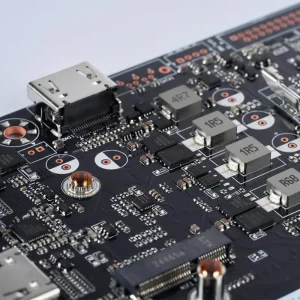
High-frequency substrates featuring tight impedance control for RF transceivers and base stations.
View Details →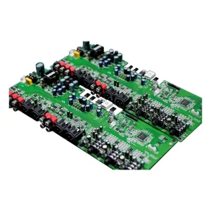
Heavy-copper PCBs engineered for high-efficiency power conversion and robust thermal dissipation.
View Details →Get in touch with our engineering team today for a comprehensive DFM review and a competitive quote for your next PCBA production run.
Send Inquiry Now