Engineered for local smart industry, automated logistics hubs, and advanced security networks across Singapore
Mapping the intersections of Global Value Chains (GVCs), local R&D hubs, and advanced prototyping requirements in Southeast Asia's tech capital
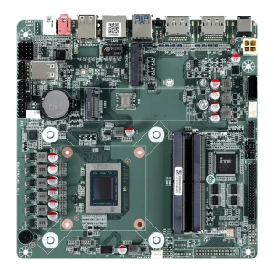
Singapore occupies a pivotal position in the global semiconductor and electronics manufacturing value chain. As a leading hub for advanced electronics, the nation-state accounts for roughly 11% of the global semiconductor market and 20% of global semiconductor equipment manufacturing. With the rapid expansion of Industry 4.0, IoT applications, Smart Nation initiatives, and advanced MedTech clusters, the demand for high-reliability Printed Circuit Board Assembly (PCBA) has transformed from mass-market production to agile, precision-focused High-Mix, Low-Volume (HMLV) manufacturing.
Local Singaporean enterprises, multinational R&D headquarters located in the Science Park and JTC LaunchPad, and specialized engineering firms require a seamless transition from prototype validation to localized market deployment. The integration of aerospace avionics, high-frequency communication protocols (5G/6G), medical device diagnostic boards, and automotive grade EV assemblies requires a manufacturing partner operating strictly under international control systems such as IATF 16949 for automotive, ISO 13485 for medical, and IPC-A-610 Class 3 standards for aerospace and critical defense hardware.
Furthermore, Singapore’s strict regulatory policies regarding environmental sustainability (such as the Singapore Green Plan 2030) push PCBA application standards towards lead-free (RoHS compliant) manufacturing, high thermal efficiency, and minimal electrostatic discharge (ESD) risks. Electronics manufacturers must integrate advanced engineering insights directly into their design phases to ensure maximum structural integrity and component traceability.
Empowering Global Innovation Through High-Precision Electronics Manufacturing Services
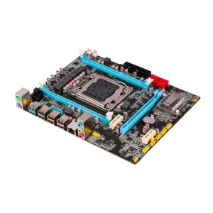
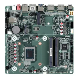
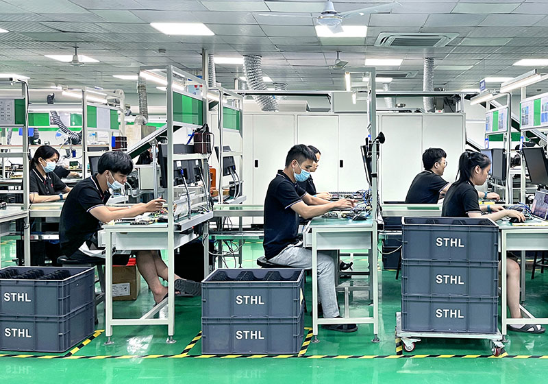
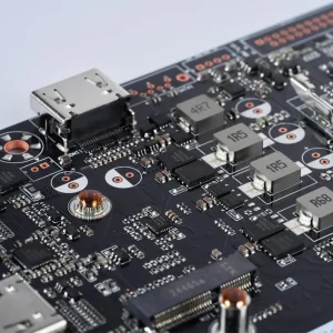
Shenzhen STHL is a premium provider of electronics manufacturing services (EMS) in China, serving customers worldwide along the entire industry chain. Our capabilities span across PCB layout design, electronic component sourcing, PCB fabrication, PCBA assembly, custom cable assembly, complete box build assembly, and comprehensive functional testing services.
Established in 2006, STHL has built over 20 years of experience in electronics contract assembly manufacturing. Our operations now support over 220 skilled engineering and manufacturing staff members, ensuring top-tier service output for projects scaling from quick-turn prototyping to mass production runs.
We supply advanced hardware assemblies to customers across the USA, Germany, Italy, UK, Poland, New Zealand, Argentina, Brazil, Turkey, Korea, Thailand, and more than 90 other regions around the globe, bridging the distance with transparent communication and robust logistics.
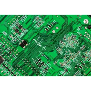
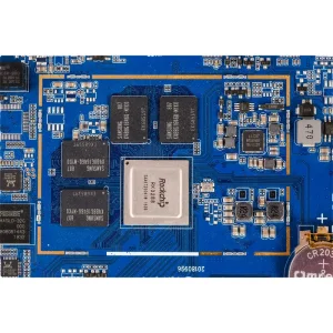
Our advanced Surface Mount Technology (SMT) lines are designed to handle complex, high-density component placements down to ultra-fine pitches. We possess the machinery and engineering depth to place and inspect:
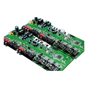
For applications requiring massive mechanical strength, extreme thermal endurance, or high power inputs, our Through-Hole Technology (THT) lines provide high-reliability manual and automated insertion services:
End-to-end engineering support designed to fast-track product delivery and secure supply chains
Operates 7 automated PCB assembly lines handling prototypes and high-volume mass production. Multi-stage quality checkpoints ensure zero-defect assembly.
Production of high-layer rigid, flex, and rigid-flex printed circuit boards using high-Tg materials designed for harsh industrial applications.
Global electronic component sourcing backed by rigid counterfeiting prevention. Access to direct OCM/distributor networks ensures stable production runs.
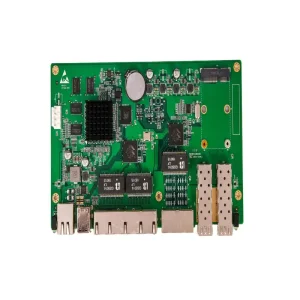
Precision cable and wire harness manufacturing. Full customization of shielded systems, connector types, strain reliefs, and custom overmolding.
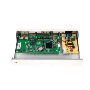
Complete mechanical enclosure integration, cable routing, display mountings, thermal solution assembly, and shipping-ready commercial packaging.
Advanced diagnostic checks including In-Circuit Testing (ICT), software flashing, RF calibration, and thermal cycling for hardware validation.
How advanced electronics manufacturing technologies align with modern semiconductor and hardware trends
Transitioning from 0201 passive components to 01005 and sub-millimeter silicon-level wafer-scale packaging (WLCSP).
Deployment of multi-layer blind and buried microvias, arbitrary layer stack-ups, and embedded passive components for 5G applications.
Integration of metal-core substrates (MCPCBs), advanced thermal paste/pad application, and copper coin insertion for EV high-power circuits.
Integrating real-time algorithmic AOI processing to predict solder joint failure rates and automatically modify reflow profiles.
Adapting advanced PCBA techniques to target specific industries driving Singapore's technological growth
Singapore is home to some of the world's most automated shipping terminal hubs. Industrial-grade automated guided vehicles (AGVs), sorting crane controllers, and automated warehousing systems require heavy-duty PCBA controllers. These boards must withstand continuous vibrational shock, high humidity, and extreme thermal cycling while maintaining reliable CAN bus communications and power conversion efficiency.
With major medical global companies centering their engineering departments in Singapore, compliance with ISO 13485 standards is essential. We manufacture high-reliability PCBs for diagnostic imaging machines, patient monitoring systems, and wearable health IoT devices. These units require zero lead contamination, pristine signal shielding, and micro-amp level current control.
Singapore is a premier aerospace maintenance, repair, and overhaul (MRO) center in the Asia-Pacific. Avionics controllers, cabin flight communication gear, and environmental control boards demand IPC Class 3 manufacturing standards. Our rigorous testing services—including environmental stress testing and 3D X-Ray checkouts—ensure that micro-components perform flawlessly in high-altitude environments.
Singapore's Smart Nation initiative requires millions of interconnected sensor nodes for environmental monitoring, smart traffic routing, and grid management. These small-form IoT devices rely on RF communication modules, Bluetooth Low Energy (BLE), and ultra-low power microcontrollers. Our precision SMT lines handle trace-level RF tuning and automated silicone conformal coating to protect devices from regional humidity.
Technical answers resolving key inquiries regarding component procurement, manufacturing yields, and reliability protocols
We work exclusively with authorized global distributors (such as Mouser, DigiKey, Arrow, and Avnet) and direct component manufacturers. For client-sourced or hard-to-find parts, we run comprehensive quality verification, including microscopic analysis, X-Ray analysis, and electrical testing to guarantee authenticity before production begins.
We perform 3D Solder Paste Inspection (SPI) on our printing lines to check paste volume and alignment. Following placement and reflow, all BGA boards undergo Automatic Optical Inspection (AOI) alongside real-time 2D/3D X-Ray inspections to confirm voiding standards meet IPC-A-610 Class 3 specifications.
Yes. We run dedicated Lead-Free SMT lines with specialized reflow profiles engineered for high-temperature SAC305 and SAC0307 alloys. Every assembly complies fully with RoHS standards, which is a key requirement for electronics used in Singapore green building projects and public utilities.
Quick-turn prototyping can be completed in 3 to 7 working days once all PCB files and components are ready. Standard production volumes vary from 2 to 4 weeks depending on the complexity of the design, custom testing requirements, and enclosure assembly (box build) specifications.
We require standard ODB++ or Gerber RS-274X layout files, an organized Bill of Materials (BOM) in Excel format (including manufacturer part numbers, descriptions, and quantities), and Centroid (Pick-and-Place) coordinates for accurate automated alignment.
Yes, our engineering team performs a thorough DFM and DFT check on every project. We analyze trace clearance, component spacing, thermal relief, pad designs, and test point accessibility to reduce production risks and avoid unexpected manufacturing costs.
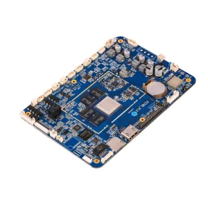
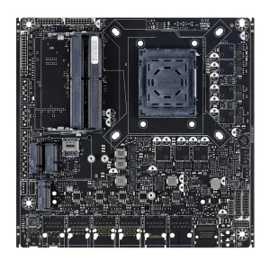
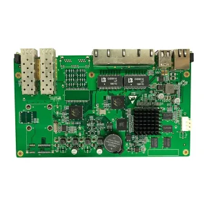
Explore our specialized assemblies designed for telecommunications, green energy, automotive, and consumer technology markets
Whether you require a quick-turn SMT prototype, design validation, or multi-layer box build assemblies, our engineers are ready to support your business requirements in Singapore and worldwide.
Send Inquiry Now