1 / 1
Early challenges in battery charger adoption—such as weak charging signal capture, electromagnetic interference (EMI), and poor electrical safety isolation in high-voltage operation—have been overcome by specialized PCB assembly technologies, particularly high-efficiency rigid PCBs and high-precision surface mount technology (SMT). These innovations effectively enhance the sensitivity of analog front-ends for capturing faint charging current and voltage signals, while integrating EMI shielding layers to eliminate interference from external power grids and electronic devices. High-efficiency rigid PCBs, in particular, balance compact form factors with reliable power and signal transmission, supporting the miniaturization of portable and desktop battery chargers without compromising charging efficiency. This technological leap has enabled battery charger PCB assemblies to outperform traditional charging circuits in key areas:
Early challenges in radiation detector adoption—such as weak radiation signal capture, electromagnetic interference (EMI), and poor radiation resistance in harsh environments—have been overcome by specialized PCB assembly technologies, particularly low-noise rigid-flex PCBs and high-precision surface mount technology (SMT). These innovations effectively enhance the sensitivity of analog front-ends for capturing faint radiation-induced electrical signals (from gamma, X-ray, and beta rays), while integrating multi-layer EMI shielding layers to eliminate interference from external electronic equipment and ambient radiation. Low-noise rigid-flex PCBs, in particular, balance compact form factors with reliable signal transmission, supporting the miniaturization of portable and handheld radiation detectors without compromising detection accuracy. This technological leap has enabled radiation detector PCB assemblies to outperform traditional detection circuits in key areas:
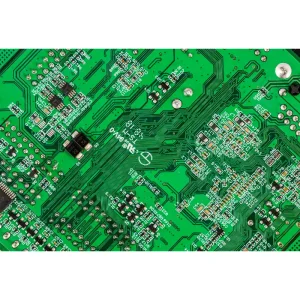
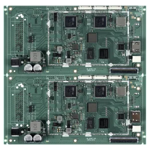
Early challenges in BMS adoption—such as weak battery cell signal capture, electromagnetic interference (EMI), and poor safety isolation in high-current scenarios—have been overcome by specialized PCB assembly technologies, particularly high-density rigid PCBs and high-precision surface mount technology (SMT). These innovations effectively enhance the sensitivity of analog front-ends for capturing faint cell voltage, current, and temperature signals, while integrating EMI shielding layers to eliminate interference from battery packs and external power equipment. High-density rigid PCBs, in particular, balance compact form factors with reliable signal transmission, supporting the miniaturization of BMS modules without compromising performance. This technological leap has enabled BMS PCB assemblies to outperform traditional battery monitoring circuits in key areas:
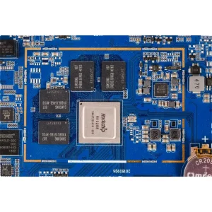
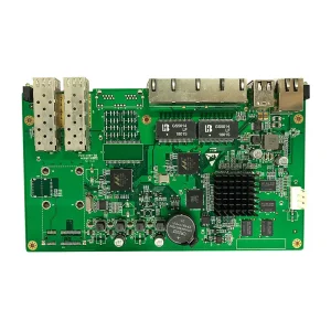
Early challenges in sensor adoption—such as weak signal capture from low-output sensors, electromagnetic interference (EMI), and poor compatibility with diverse sensor types—have been overcome by specialized PCB assembly technologies, particularly high-density HDI PCBs and high-precision surface mount technology (SMT). These innovations effectively enhance the sensitivity of analog front-ends for capturing faint sensor signals, while integrating EMI shielding layers to eliminate interference from industrial equipment and environmental factors. HDI PCBs, in particular, balance compact form factors with reliable multi-channel signal transmission, supporting the miniaturization of integrated sensor modules without compromising data accuracy. This technological leap has enabled sensors PCBA assemblies to outperform traditional sensor circuits in key areas:
Early challenges in digital X-ray machine adoption—such as high-voltage breakdown risks, electromagnetic interference (EMI) during flat-panel detector (FPD) data acquisition, and the dilemma of balancing compact device design with stable operational performance—have been overcome by specialized PCB assembly technologies, particularly multilayer HDI PCBs and high-precision surface mount technology (SMT). These innovations effectively enhance the voltage tolerance of power control modules for X-ray generators, while integrating EMI shielding layers and low-noise signal paths to eliminate interference from mechanical components and external medical equipment. Multilayer HDI PCBs, in particular, balance high-density component integration with reliable high-speed data transmission, supporting the miniaturization of portable digital X-ray devices without compromising imaging quality. This technological leap has enabled digital X-ray machine PCB assemblies to outperform traditional control circuits in key areas:
Early challenges in ECG monitor adoption—such as weak signal capture, electromagnetic interference (EMI), and poor patient safety isolation—have been overcome by specialized PCB assembly technologies, particularly rigid-flex PCBs and high-precision surface mount technology (SMT). These innovations effectively enhance the sensitivity of analog front-ends for capturing faint cardiac electrical signals, while integrating EMI shielding layers to eliminate interference from external medical equipment. Rigid-flex PCBs, in particular, balance compact form factors with reliable signal transmission, supporting the miniaturization of portable and wearable ECG devices without compromising performance. This technological leap has enabled ECG monitor PCB assemblies to outperform traditional monitoring circuits in key areas:
They address critical issues including weak charging signal capture, electromagnetic interference (EMI), and poor electrical safety isolation during high-voltage operations by utilizing high-efficiency rigid PCBs and high-precision SMT.
They enhance the sensitivity of analog front-ends to capture faint radiation-induced electrical signals, block external interference with multi-layer EMI shielding, and enable compact, portable detector designs.
They balance extremely compact dimensions with reliable signal transmission. This enables accurate monitoring of cell voltage, current, and temperature signals without sacrificing the overall performance of the BMS module.
HDI PCBs support high-density routing and multi-channel signal transmission, allowing for the miniaturization of integrated sensor modules while keeping data capture highly accurate and isolated from environmental noise.
They utilize multilayer HDI PCBs to increase high-voltage tolerance, incorporate EMI shielding layers to block interference during flat-panel detector data acquisition, and support high-speed data transmission for crisp imaging.
They combine structural flexibility and rigid reliability, allowing devices to remain compact and wearable while protecting sensitive analog front-ends from external EMI to capture weak cardiac signals clearly.