1 / 1
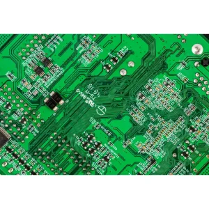
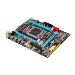
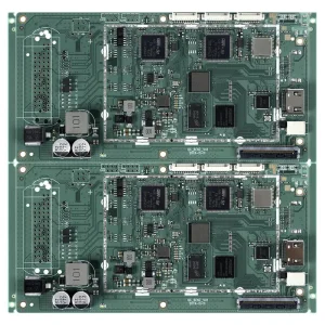
Early challenges in electric vehicle (EV) charging pile adoption—such as weak charging signal capture, electromagnetic interference (EMI), and poor safety isolation in high-voltage operation—have been overcome by specialized PCB assembly technologies, particularly ruggedized high-power PCBs and high-precision surface mount technology (SMT). These innovations effectively enhance the sensitivity of analog front-ends for capturing faint voltage, current, and communication signals, while integrating EMI shielding layers to eliminate interference from power grids and on-board vehicle electronics. Ruggedized high-power PCBs, in particular, balance compact form factors with reliable high-voltage signal transmission, supporting the miniaturization of charging pile control units without compromising charging efficiency and safety. This technological leap has enabled EV charging pile PCB assemblies to outperform traditional charging control circuits in key areas.
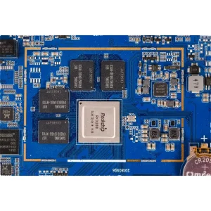
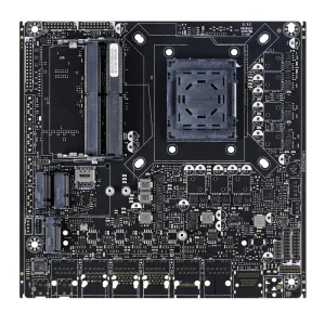
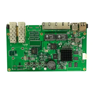
Early challenges in sensor adoption—such as weak signal capture from low-output sensors, electromagnetic interference (EMI), and poor compatibility with diverse sensor types—have been overcome by specialized PCB assembly technologies, particularly high-density HDI PCBs and high-precision surface mount technology (SMT). These innovations effectively enhance the sensitivity of analog front-ends for capturing faint sensor signals, while integrating EMI shielding layers to eliminate interference from industrial equipment and environmental factors. HDI PCBs, in particular, balance compact form factors with reliable multi-channel signal transmission, supporting the miniaturization of integrated sensor modules without compromising data accuracy. This technological leap has enabled sensors PCBA assemblies to outperform traditional sensor circuits in key areas.
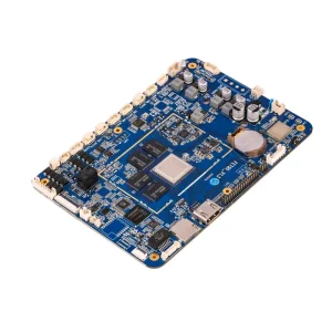
Early challenges in digital X-ray machine adoption—such as high-voltage breakdown risks, electromagnetic interference (EMI) during flat-panel detector (FPD) data acquisition, and the dilemma of balancing compact device design with stable operational performance—have been overcome by specialized PCB assembly technologies, particularly multilayer HDI PCBs and high-precision surface mount technology (SMT). These innovations effectively enhance the voltage tolerance of power control modules for X-ray generators, while integrating EMI shielding layers and low-noise signal paths to eliminate interference from mechanical components and external medical equipment. Multilayer HDI PCBs, in particular, balance high-density component integration with reliable high-speed data transmission, supporting the miniaturization of portable digital X-ray devices without compromising imaging quality. This technological leap has enabled digital X-ray machine PCB assemblies to outperform traditional control circuits in key areas.
Early challenges in ECG monitor adoption—such as weak signal capture, electromagnetic interference (EMI), and poor patient safety isolation—have been overcome by specialized PCB assembly technologies, particularly rigid-flex PCBs and high-precision surface mount technology (SMT). These innovations effectively enhance the sensitivity of analog front-ends for capturing faint cardiac electrical signals, while integrating EMI shielding layers to eliminate interference from external medical equipment. Rigid-flex PCBs, in particular, balance compact form factors with reliable signal transmission, supporting the miniaturization of portable and wearable ECG devices without compromising performance. This technological leap has enabled ECG monitor PCB assemblies to outperform traditional monitoring circuits in key areas.
A1: Modern PCB assemblies incorporate dedicated EMI shielding layers and high-precision surface mount technology (SMT). These enhancements effectively block electromagnetic interference originating from both the power grid and nearby on-board vehicle electronics, ensuring stable signal transmission.
A2: Specialized multilayer HDI PCBs and advanced SMT techniques are utilized to significantly improve the voltage tolerance of power control modules. Additionally, these technologies isolate high-voltage paths to prevent breakdown risks while maintaining a compact device profile.
A3: Rigid-flex PCBs offer a unique balance of mechanical flexibility and component density. They enable reliable, low-noise transmission of faint cardiac electrical signals across compact, space-constrained wearable formats without sacrificing safety or signal sensitivity.
A4: High-density interconnect (HDI) technology allows for compact routing and minimal signal loss across multiple channels. This configuration effectively preserves the integrity of faint sensor signals against industrial noise and external environmental factors.
A5: High-precision surface mount technology (SMT) facilitates the placement of micro-components with tight tolerances. This allows for miniaturized control boards, improved thermal dissipation, and enhanced reliability under high-voltage, high-power operating conditions.