1 / 1
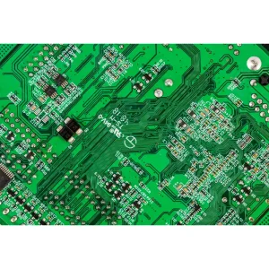
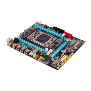
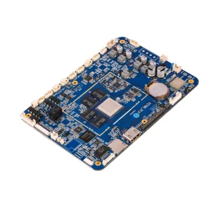
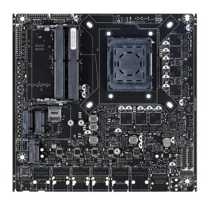
Early challenges in smart lock adoption—such as weak signal capture for unlock verification, electromagnetic interference (EMI), and poor balance between security and low-power operation—have been overcome by specialized PCB assembly technologies, particularly rigid-flex PCBs and high-precision surface mount technology (SMT). These innovations effectively enhance the sensitivity of analog front-ends for capturing faint verification signals (including fingerprint, Bluetooth, NFC, and UWB signals), while integrating EMI shielding layers to eliminate interference from external electronic devices and environmental factors. Rigid-flex PCBs, in particular, balance compact form factors with reliable signal transmission, supporting the miniaturization of smart lock devices without compromising security performance and response speed. This technological leap has enabled smart lock PCB assemblies to outperform traditional lock circuits in key areas:
High-sensitivity analog front-ends allow seamless capturing of faint verification signals such as fingerprint, Bluetooth, NFC, and UWB.
Integrated shielding layers eliminate interference from surrounding electronic systems and unpredictable environmental factors.
Rigid-flex PCBs balance compact physical footprints with highly reliable signal transmission channels, maintaining peak response speed.
Early smart locks struggled with weak signal capture for unlock verification, high vulnerability to electromagnetic interference (EMI), and finding a balance between security operations and low-power efficiency.
High-precision surface mount technology (SMT) optimizes the layout of analog front-ends, enhancing their overall sensitivity to accurately capture faint signals like fingerprints, Bluetooth, NFC, and UWB.
Rigid-flex PCBs balance extremely compact, space-saving designs with highly reliable high-speed signal transmissions, allowing smart locks to remain small yet fully secure.
Advanced PCB designs integrate specialized, multi-layer EMI shielding blocks that block out external noise from neighboring electrical appliances and environment factors.
No. Thanks to high-density SMT layouts and rigid-flex PCB substrates, device miniaturization is achieved without causing any delays or reductions in security verification speeds.