1 / 1
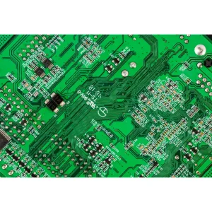
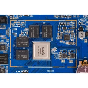
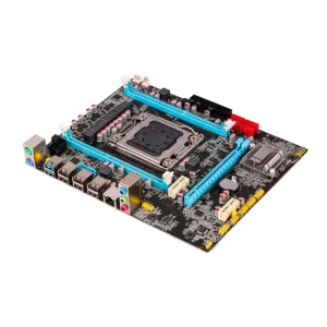
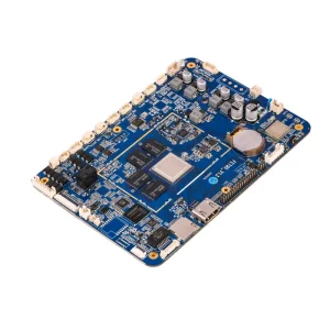
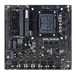
Early challenges in wireless signal booster adoption—such as weak base signal capture, severe broadband electromagnetic interference (EMI), and insufficient high-frequency circuit safety isolation—have been overcome by specialized PCB assembly technologies, particularly rigid-flex PCBs and high-precision surface mount technology (SMT). These innovations effectively enhance the sensitivity of analog front-ends for capturing faint wireless network electrical signals, while integrating multi-layer high-frequency EMI shielding layers to eliminate interference from household appliances, industrial equipment and overlapping network signals. Rigid-flex PCBs, in particular, balance compact miniaturized form factors with stable high-gain signal transmission, supporting the lightweight design of wireless signal boosters without compromising signal amplification efficiency and network stability. This technological leap has enabled wireless signal booster PCBA assemblies to outperform traditional signal amplification circuits in key areas:
Enables the capturing of exceptionally faint wireless network electrical signals to maximize amplification efficiency.
Eliminates interference from household appliances, industrial gear, and overlapping communication networks.
Combines a compact, lightweight physical structure with robust high-gain signal routing and thermal reliability.