High-Quality Smartphone PCBA Assembly--STHL Manufacturers, Factories

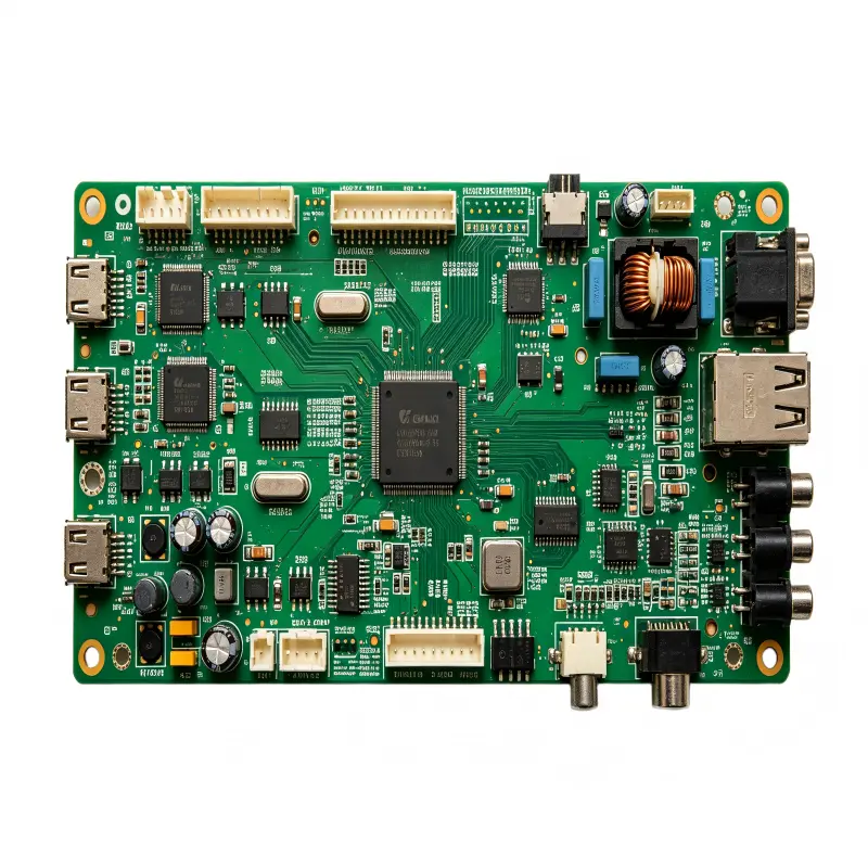
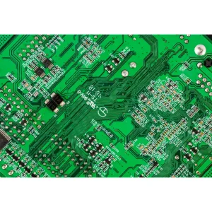
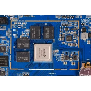
Custom high-precision PCBA assembly solutions specifically designed for smartphones, integrating high-density placement and miniaturized component packaging technology. As the "neural center" of the smartphone, it is responsible for signal transmission and energy management of core modules such as processors, image modules, and radio frequency systems. With over 19 years of manufacturing experience, we achieve precise soldering of millimeter-level components and anti-interference layout, ensuring smooth operation of all scenarios including calls, imaging, and fast charging, and adapting to the differentiated production needs of high-end flagship phones and mid-range mass-produced phones.

Product Description

Smartphone PCBA Assembly

Early challenges in smartphone adoption—such as unstable radio frequency signal reception, severe electromagnetic interference (EMI), and insufficient internal circuit safety isolation—have been overcome by specialized PCBA assembly technologies, particularly high-density rigid-flex PCBs and ultra-precision surface mount technology (SMT). These innovations effectively enhance the sensitivity of analog front-ends for capturing faint communication and sensing electrical signals, while integrating multi-layer EMI shielding structures to eliminate interference between internal chips, camera modules and wireless components. Rigid-flex PCBs, in particular, balance ultra-thin compact form factors with high-speed signal transmission, supporting the thinning and structural miniaturization of modern smartphones without compromising overall device performance. This technological leap has enabled smartphone PCBA assemblies to outperform traditional mobile circuit boards in key areas:
Key Technical Advantages
  • High-Density Rigid-Flex PCBs: Balances ultra-thin compact form factors with high-speed signal transmission.
  • Ultra-Precision SMT: Enhances the sensitivity of analog front-ends for capturing faint communication and sensing electrical signals.
  • Multi-Layer EMI Shielding: Integrates structures to eliminate interference between internal chips, camera modules, and wireless components.
  • Structural Miniaturization: Supports thinning and layout optimization without compromising overall device performance.

Frequently Asked Questions

What were the early challenges in smartphone PCBA designs?
Early smartphone designs faced issues like unstable radio frequency signal reception, severe electromagnetic interference (EMI), and insufficient internal circuit safety isolation.
How do rigid-flex PCBs benefit modern smartphone structures?
Rigid-flex PCBs balance ultra-thin compact form factors with high-speed signal transmission, supporting structural thinning and miniaturization without compromising performance.
How is electromagnetic interference (EMI) resolved in PCBA assembly?
EMI is resolved by integrating multi-layer EMI shielding structures into the PCB design, which eliminates interference between internal chips, wireless components, and camera modules.
What role does ultra-precision SMT play in smartphone boards?
Ultra-precision Surface Mount Technology (SMT) enables accurate placement of components, effectively enhancing the sensitivity of analog front-ends to capture faint communication and electrical signals.
Do advanced PCBA assemblies affect the overall device safety?
Yes, specialized PCBA assembly technologies provide advanced circuit safety isolation alongside high-density integration, resolving historical circuit stability issues.

Related Products