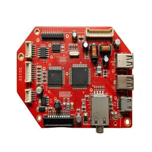
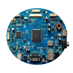
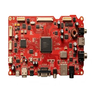
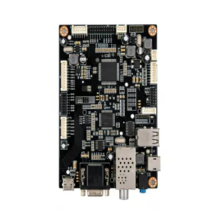
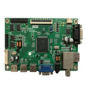
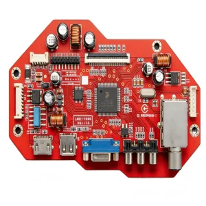
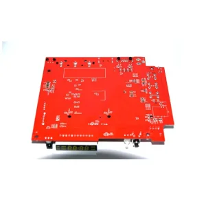
Explore our industrial-grade, certified PCBA assemblies engineered for high stress, extreme reliability, and structural durability.
Understanding the tectonic shifts in electronics manufacturing and the requirement for high-integrity contract assembly.
Modern commercial and industrial hardware ecosystems demands unprecedented precision. As microprocessors scale down and operating frequencies climb into the gigahertz range, PCBA (Printed Circuit Board Assembly) has ceased to be a simple mounting platform. It is now a critical, active element of circuit performance, electromagnetic compatibility (EMC), and thermal dissipation.
Global markets, notably in the USA, Germany, Italy, UK, and Japan, are transitioning toward dense, multi-layer designs that require zero-defect manufacturing. Key performance indicators are no longer limited to assembly cost, but rather evaluate structural integrity, functional lifetime under extreme thermal cycling, and compliance with severe environmental regulations.
From consumer-grade rapid prototyping to high-reliability long-lifecycle industrial systems. High-reliability applications, such as automotive radar modules, aerospace flight control platforms, and medical diagnostic instruments, cannot tolerate field failures. A single solder joint failure can disrupt logistics, breach safety protocols, or cause catastrophic system shutdowns.
Addressing the core requirements of sourcing directors: quality controls, counterfeit prevention, and component traceability.
Procuring raw components requires absolute protection against counterfeit parts. Enterprises demand complete chain-of-custody documentation, original manufacturer OCM certificates, and visual/parametric testing protocols to ensure every IC, capacitor, and sensor is genuine.
Engineering teams need pre-production reviews. DFM optimization identifies thermal traps, via-in-pad defects, footprint mismatches, and board-edge clearance issues before the physical tooling process begins, reducing iterations and development costs.
Managing raw material supply chains requires deep intelligence. Leading EMS factories mitigate long lead times by suggesting alternative footprints, dual-source active components, and securing raw laminates to guarantee on-time delivery despite market volatility.
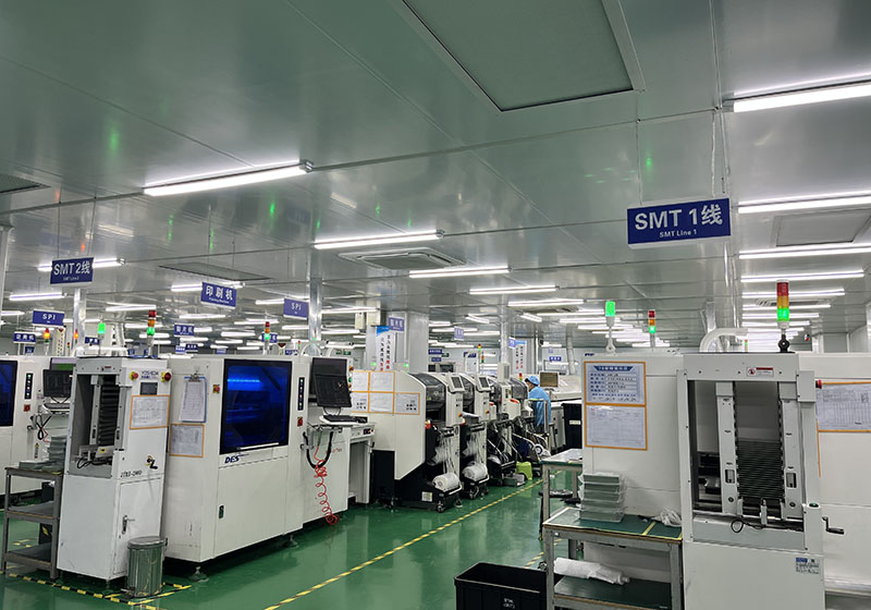
A look inside our 10,000 sqm production facility optimized for advanced electronics contract manufacturing.
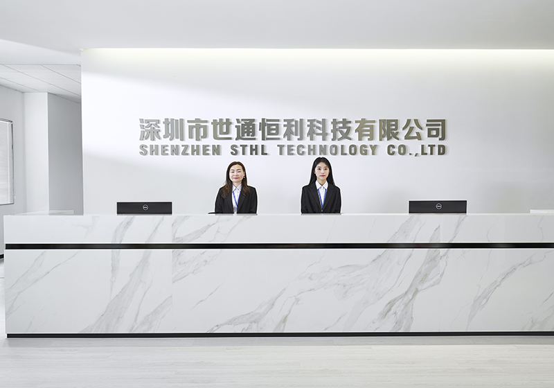
Shenzhen STHL has established itself as an electronics manufacturing services (EMS) provider in China. Supporting a diverse international client base spanning over 90 regions, we provide turnkey engineering coverage from initial PCB layout and component sourcing to multi-layered fabrication, precision assembly, cable integration, complete box builds, and advanced functional testing.
Our operations are designed to satisfy international standards. Our manufacturing workflow is certified under IATF 16949 (Automotive), ISO 13485 (Medical), ISO 9001 (Quality Management), and ISO 14001 (Environmental). This structural compliance guarantees that every board shipped complies with international RoHS regulations, offering durability under stressful environments.
By coupling advanced manufacturing hardware with automated quality control check-points, STHL offers low defect rates (measured in DPPM), making us a reliable partner for Tier-1 engineering firms.
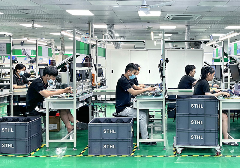
An overview of our mechanical and chemical engineering capabilities across Surface Mount and Through-Hole Technologies.
STHL specializes in processing complex, high-pin-count BGA and micro-BGA (uBGA) components. We manage placement down to 0.3mm pitch, utilizing real-time 3D Solder Paste Inspection (SPI) to avoid solder-bridging, voiding, or cold joints. Solder joint integrity under these components is confirmed post-reflow using advanced transmission X-Ray inspection.
Our placement platforms manage complex packaging geometries, including Package-on-Package (PoP), QFN, QFP, and ultra-miniature passive components (down to 01005 footprints). Precision placement machines use vision alignment systems to monitor offsets in real-time, preventing layout defects.
For high-power, high-vibration applications requiring structural lead joints, STHL maintains dedicated THT (Through-Hole Technology) lines. Combining manual insertions and wave soldering machinery, we secure mechanical connections. Process designs use wave soldering fixtures to protect SMT components on double-sided boards.
At STHL, quality control is integrated into every step of the line. The process begins with 3D Solder Paste Inspection (SPI), which checks paste volume, registration, and height profile before component placement. Post-reflow, boards pass through high-definition Automated Optical Inspection (AOI) to identify defects like tombstoning, insufficient solder, or polarity errors.
For hidden solder interfaces (BGA and QFN thermal pads), we perform high-resolution X-Ray Inspection to detect voiding and micro-fractures. We also offer In-Circuit Testing (ICT) and customized Functional Testing (FCT), verifying the electrical and signaling behaviors of the final product under load simulations.
Tailored manufacturing, engineering, and compliance configurations across diversified industrial domains.
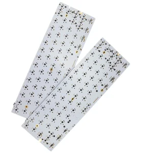
High-vibration, thermal-cycle resistant PCBAs for ADAS, millimeter-wave radar modules, engine controllers, and LED lighting assemblies. We utilize low-voiding solder alloys, thermal paste dispensing, and conformal coatings to prevent oxidation, degradation, and trace-bridging under high under-hood temperatures.
Class II and Class III PCBA production, including portable ultrasound electronics, diagnostic monitors, and wearable health trackers. Every production batch undergoes tracking, component-level traceability, and strict ESD controls to meet medical safety standards.
Rugged, heavy-copper PCB designs and assemblies engineered for solar power inverters, wastewater monitoring systems, and flight computer hardware. We support high-reliability operation under variable loads, corrosive atmospheres, and high-voltage conditions.
How STHL adapts to the future of high-density interconnects, IoT scaling, and automated assembly.
As the Internet of Things (IoT), 5G telecommunications, and Edge Artificial Intelligence drive components closer together, traditional substrate limits are being reached. Our technology roadmap addresses these trends by refining HDI (High-Density Interconnect) manufacturing processes. This includes micro-via drilling, blind/buried vias, and advanced laser routing to maximize signal integrity while minimizing board area.
We are also upgrading our lines to support high-frequency substrates (such as Rogers, Taconic, and Nelco laminates) for next-generation RF applications. These include Millimeter-wave radar sensors and 5G transceiver stations. Additionally, our chemical engineering team is developing lead-free, halogen-free surface finishes (such as ENIG, ENEPIG, and OSP) to support eco-friendly regulations and improve joint reliability in high-vibration environments.
Ensuring smooth cross-border delivery, trade compliance, and reliable quality guarantees.
STHL operates under international quality frameworks. Our compliance certificates include:
Our production floor features continuous electrostatic discharge (ESD) monitoring, humidity-controlled storage for raw PCBs and sensitive components (MSL tracking), and HEPA-filtered air circulation systems. This setup protects sensitive silicon components from electrostatic discharge and moisture-induced defects during reflow.
We manage shipping logistics for clients worldwide. Using custom packaging, ESD shielding bags, vacuum-sealed containers, and drop-tested boxes, we ensure our assemblies arrive safely. Our team handles custom clearance, documentation, and tax declarations for smooth transport into Europe, North America, and Asia.
Answers to common questions regarding PCBA manufacturing, engineering procedures, and procurement logistics.
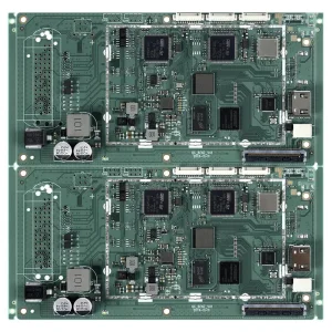
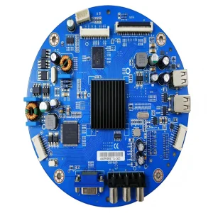
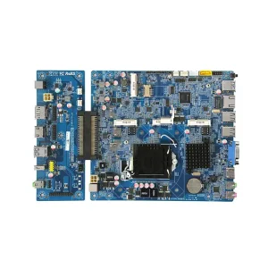
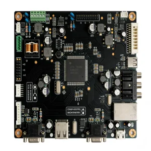
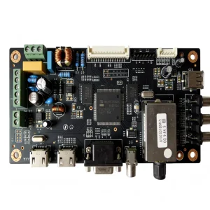
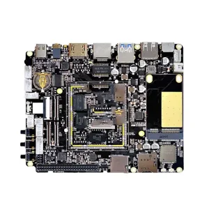
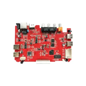
Explore our specialized boards engineered for lighting systems, industrial print engines, and high-performance flight controllers.