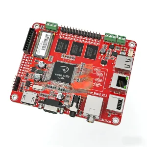
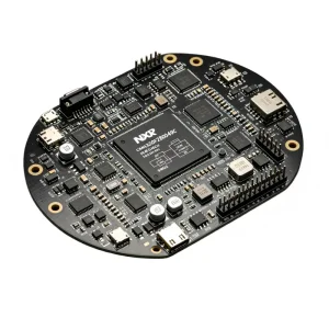
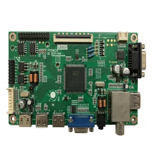
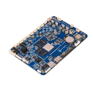
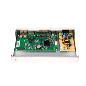
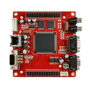
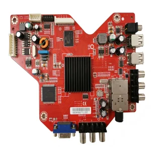
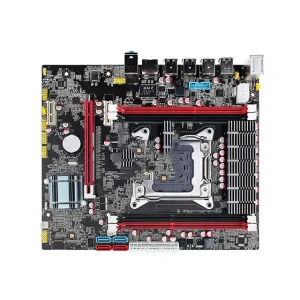
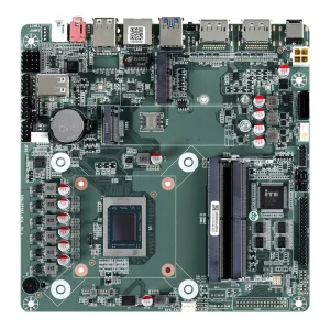
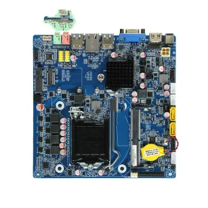
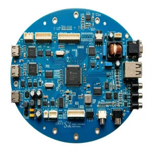
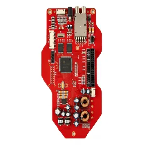
Explore our core medical, industrial, power, and smart monitoring assemblies engineered to meet rigorous high-density specifications.
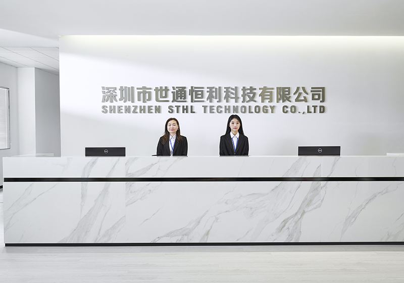
Shenzhen STHL stands as a premiere high-quality provider of electronics manufacturing services (EMS) in China. We serve customers worldwide along the whole industry chain, encompassing professional PCB layout optimization, global components sourcing, high-density PCB fabrication, SMT and THT assembly, cable assembly, complex box build, and comprehensive functional testing services.
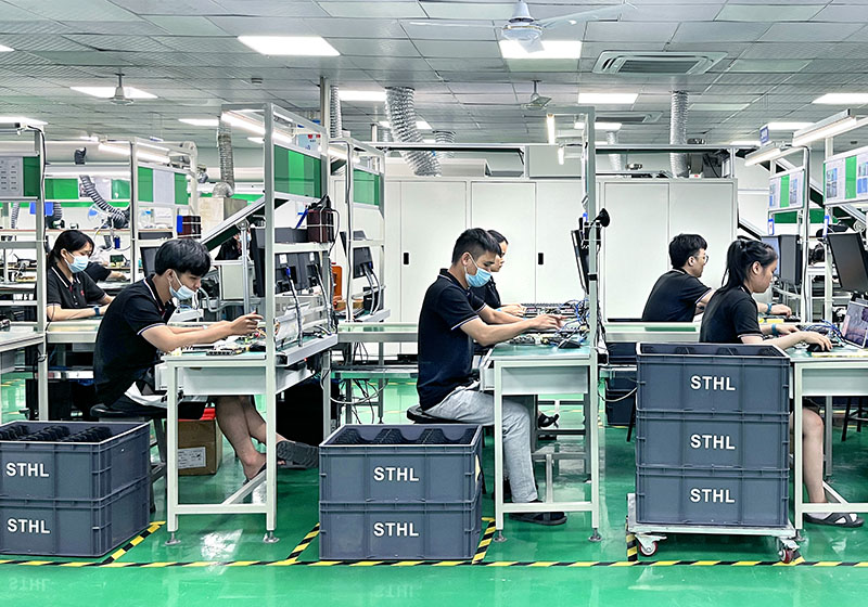
Established in 2006, STHL brings 20 years of expertise to electronics contract assembly manufacturing. Our modern, 10,000 sqm facilities host 220+ technical staff members and operate 7 SMT assembly lines, 2 DIP/THT lines, 2 function testing lines, and 2 finished device assembly lines. This capacity allows us to pivot rapidly from high-density rapid-prototyping to volume production runs.
We deliver certified electronic assembly services across multiple critical domains, including automotive (IATF 16949), medical devices (ISO 13485), energy power, aerospace, IoT, and communications. Today, STHL is trusted as a long-term reliable vendor by clients in the USA, Germany, Italy, the UK, Poland, New Zealand, Argentina, Brazil, Turkey, Korea, Thailand, and over 90 regions globally. All our processes align with RoHS and REACH environmental guidelines to guarantee global compliance.
Maximizing signal integrity and component density through advanced thermal profiles, precision tooling, and high-resolution optical inspections.
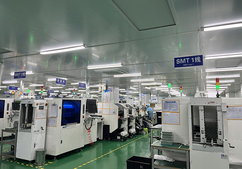
Modern circuits demand high component densities. Our SMT production lines are calibrated to place complex micro-footprint parts with extreme accuracy. Our core competencies include:
For applications subject to extreme thermal and physical stress, Through-Hole Technology remains critical. Our THT lines feature:
A technical dive into microvia structures, multilayer registration, and advanced substrates driving next-generation electronic design.
Conventional vias limit signal routing space. Our fabrication capabilities support laser-drilled blind and buried microvias down to 0.075mm. By leveraging ultraviolet (UV) and carbon dioxide (CO2) lasers, we achieve precise aspect ratios (typically 1:1) to ensure excellent copper-plating deposition and reliable signal transitions across inner layers.
For smart devices requiring dense configurations, we specialize in Any-Layer ELIC (Every Layer Interconnect) stackups. By stacked microvias filled with solid copper plating (via-in-pad technology), we eliminate space-wasting breakout channels. We support build-up configurations such as 1+N+1, 2+N+2, and complex Any-Layer stacks for high-speed routing.
To reduce signal attenuation at frequencies up to 77GHz, we work with specialized high-speed/low-loss dielectrics (e.g., Rogers, Megtron 6, Isola, and Shengyi). These materials minimize dielectric constants (Dk) and dissipation factors (Df), ensuring clean signal transitions, excellent impedance control, and reliable thermal dissipation in harsh environments.
From CAD layout optimization and raw board fabrication to final box build and validation, we cover every step of the PCB lifecycle.
STHL operates 7 automated PCB assembly lines for both prototype development and volume production runs. Advanced Yamaha/Panasonic pick-and-place equipment ensures precise component placement, complemented by RoHS-compliant lead-free wave and reflow soldering.
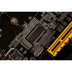
Our PCB manufacturing capabilities scale from simple single-sided designs to complex multi-layer rigid, flexible, and rigid-flex configurations. By utilizing controlled processes and premium materials, we build boards that match your exact performance requirements.
We provide global electronic component sourcing and supply chain solutions. Our broad supplier network and expertise secure genuine, certified parts, helping to mitigate risks from counterfeit components, market allocations, and long lead times.
We manufacture precision custom cable and wire harness assemblies, including connectors, handles, retention systems, and specialized shielding. Our cable assemblies support multiple configurations and are built to perform reliably in demanding industrial environments.
We offer cost-effective, full box-build integration services to help speed your products to market. Our team handles everything from placing the PCBA in its enclosure to routing internal wiring, performing final function tests, and packaging finished units.
Our team conducts comprehensive functional testing (FCT), circuit verification, boundary scans, and environmental simulation to detect defect escapes. Testing before shipment helps ensure that your products arrive stable and fully validated.
Aligning manufacturing capabilities with the strict regulatory standards and performance expectations of global technology markets.
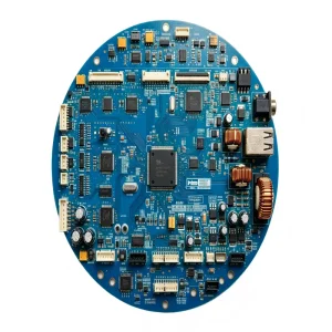
Medical electronics, like ventilators and diagnostic devices, require long-term operational stability and compliance. STHL maintains an ISO 13485 certification, implementing rigorous verification, material traceability, and continuous process monitoring. Our class-3 cleanroom environments help prevent contamination during SMT placement, ensuring components perform reliably in life-critical situations.
With the rise of electric vehicles and smart driving assistance systems, modern automotive sub-assemblies operate under high vibrations and thermal extremes. We adhere to IATF 16949 standards, using thermal shock testing, automated optical inspection, and conformal coatings to help ensure electronics remain reliable throughout their operating life.
High-power battery chargers and BMS layouts must manage high currents and dissipation effectively. Our fabrication services include heavy copper traces, custom heat sinks, and thermal vias. These features help optimize heat dissipation, reducing hot spots and improving thermal performance in power conversion systems.
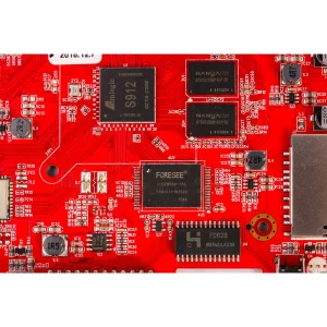
Security cameras, noise monitors, and network modems require compact form factors and reliable signal integrity. We utilize multi-layer HDI configurations to reduce EMI, control signal cross-talk, and support high-frequency communications for modern IoT devices.
Shenzhen sits at the heart of the global electronics supply chain, providing access to components and raw materials. STHL harnesses this ecosystem through digital manufacturing practices and automated production workflows:
By placing our manufacturing facility in Shenzhen, STHL benefits from a direct connection to major component distributors and testing centers. This location allows us to resolve design changes and engineering queries quickly, helping to accelerate time-to-market. For global businesses, this means faster development times, consistent material quality, and stable logistics pathways.
Our quality assurance program is built around international standards, ensuring electrical and physical safety for global markets.
Automotive core quality management practices to ensure durability, reliability, and safety.
Quality system requirements for medical device components, tracking raw materials to the source.
General manufacturing quality frameworks integrated with environmentally sound production methods.
Lead-free, halogen-free, and hazard-free manufacturing to ensure environmental safety.
Detailed answers to common questions about High-Density Interconnect manufacturing and assembly.
HDI (High Density Interconnect) boards utilize finer line spacing (typically <3 mils), smaller microvias (<6 mils), and blind or buried via structures. This allows designers to route high-pin-count BGA and package-on-package (PoP) ICs within a smaller footprint, improving high-speed signal transmission and thermal management compared to standard multilayer PCBs.
We use automated laser-drilling controls to verify microvia registration, and our electroplating processes are monitored to ensure uniform copper deposition. Quality checks include in-line 3D Automated Optical Inspection (AOI), high-resolution 2D and 3D X-Ray laminography to inspect BGA/uBGA solder joints, and functional testing to verify electrical continuity before shipping.
Yes, our facility is equipped to manufacture Any-Layer ELIC (Every Layer Interconnect) stackups. By stacking microvias filled with solid copper plating (via-in-pad technology), we eliminate space-wasting breakout channels. We support build-up configurations such as 1+N+1, 2+N+2, and complex Any-Layer stacks for high-speed routing.
We source components from authorized global distributors (like Arrow, DigiKey, and Mouser) or directly from component manufacturers. We maintain full traceability for all parts, and incoming batches undergo verification testing to ensure authenticity before entering our production lines.
Standard prototype assemblies can be completed in 7 to 10 working days once all design files (Gerber, BOM, and Pick-and-Place coordinates) and components are received. Production timelines vary based on component lead times and testing requirements, but we work with clients to coordinate schedules and help prevent project delays.
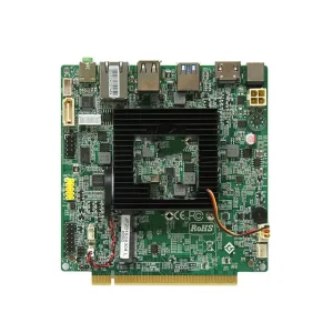
Discover our specialized battery management controllers, communication modems, and medical assemblies built to meet global safety standards.