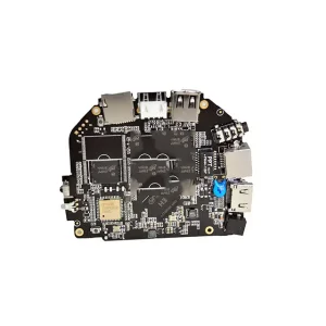
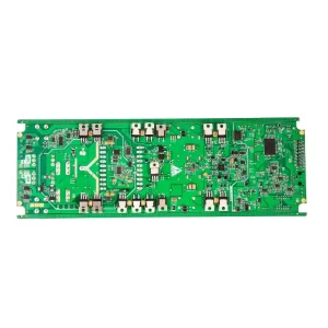
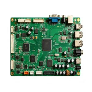
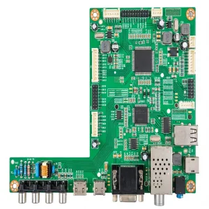
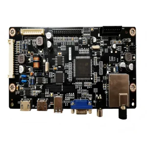
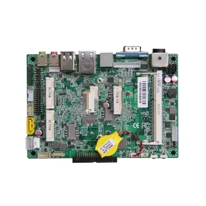
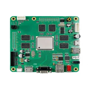
Explore our industry-standard PCBA outputs manufactured under IATF 16949, ISO 13485, and RoHS compliance paradigms.
Analyzing the shifts toward high-reliability, micro-miniaturization, and robust global logistics in modern electronics contract manufacturing.
The global commercial and industrial electronics industry is undergoing a paradigm shift. Product life cycles are contracting, while the demand for high-density, multi-functional, and ultra-reliable assembly configurations is surging. Modern manufacturing is no longer just about soldering components onto a FR-4 substrate; it is an optimized ecosystem of supply chain logistics, thermal engineering, automated inspection, and adherence to rigorous compliance frameworks.
From aerospace telemetry systems to medical diagnostics and high-voltage power grids, Printed Circuit Board Assemblies (PCBA) form the central nervous system of modern technology. Original Equipment Manufacturers (OEMs) demand a partner that offers deep engineering integration, component traceability, and automated verification systems that eliminate the risk of field failures. In this landscape, localized engineering support must run parallel with global supply chain networks to assure business continuity and cost containment.
Over 78% of warranty failures in smart devices stem from mechanical thermal mismatches near Fine-Pitch BGAs. High-quality SMT manufacturers resolve this via specialized reflow profiling and 3D X-Ray inspection.
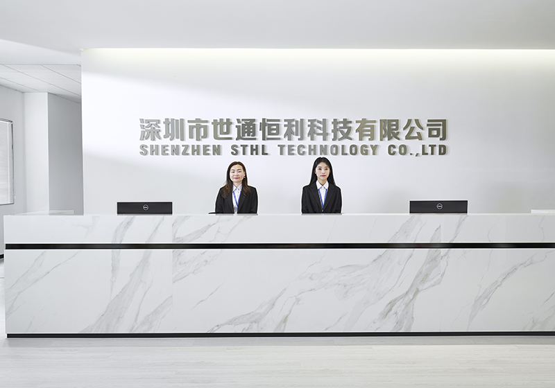
Shenzhen STHL is a high-quality provider of electronics manufacturing services (EMS) in China, serving customers worldwide across the entire industry chain.
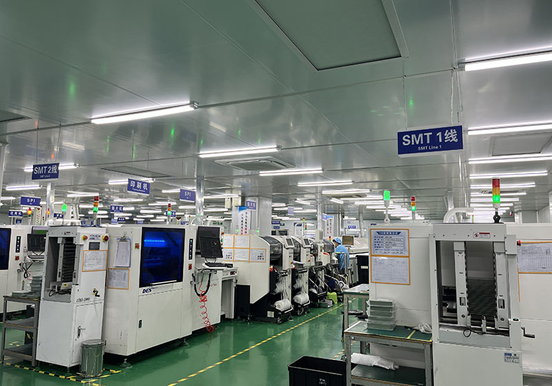
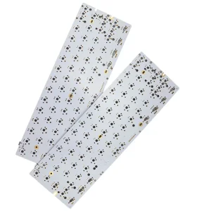
Surface Mount Technology (SMT) is the cornerstone of our high-speed, high-density assembly operations. At STHL, our engineering team optimizes component footprints, stencil apertures, and reflow profiles to process state-of-the-art packages without defects. Our lines handle:
Our commitment to defect-free execution is backed by automated inspection loops, including 3D Automated Optical Inspection (AOI) and real-time 3D X-Ray Inspection for hidden solder joints beneath BGA/QFN components.
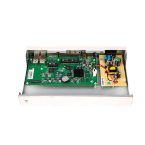
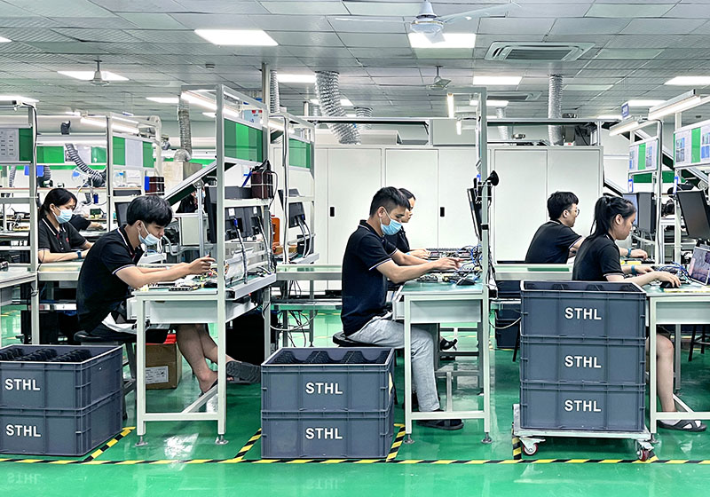
Despite the dominance of SMT, Through-Hole Technology remains indispensable for high-power interfaces, rugged mechanical connectors, and large electrolytic capacitors. STHL excels in managing dual-process (SMT + THT) hybrid assemblies utilizing:
Our specialized PCBA engineering is proven across key high-reliability sectors globally.
Manufacturing Electronic Control Units (ECUs) and Battery Management Systems (BMS). Adherence to IATF 16949 ensures vibration-resistant, high-temperature soldering profiles for functional vehicle safety.
Providing defect-free PCB assemblies for barcode scanners, physiological monitors, and clinical lab equipment. Ensuring strict component traceability and biological/chemical contamination controls.
Powering clean tech with solar inverter controller boards, industrial gas leak alarms, smart home plugs, and power quality analyzers. Our designs emphasize robust thermal management and efficient power conversion pathways.
Our 10,000 sqm ISO-certified facility provides end-to-end management from bare board fabrication to boxed delivery.
How STHL leverages Shenzhen's industrial cluster to optimize component sourcing, reduce lead times, and maintain BOM cost competitiveness.
Managing component volatility requires geographic advantages and direct manufacturer channels. Operating out of Shenzhen, the global hub of electronics hardware, STHL leverages direct factory relationships and verified distributors. This proximity dramatically reduces lead times for complex multilayer PCBs and hard-to-find active components.
Our supply chain mitigation strategy includes dual-sourcing options, real-time tracking of semiconductor allocation, and strict anti-counterfeiting validation protocols. We maintain an in-house bonded warehouse with temperature and humidity controls conforming to ESD S20.20 standards, ensuring high component yield during subsequent thermal assembly processes.
Our engineering team proactively screens your Bill of Materials (BOM) to identify end-of-life (EOL) components, recommending footprint-compatible drop-in replacements to secure production continuity.
We operate dedicated lines for quick-turn prototyping, enabling rapid design verification. DFM (Design for Manufacturing) reports are generated for every new project to catch design discrepancies early.
By consolidating material demands across global contracts, we negotiate raw material pricing directly with copper clad laminate (CCL) and semiconductor manufacturers, passing savings onto our clients.
Our transition toward Industry 4.0 Smart Manufacturing and high-density packaging capabilities.
Advanced CAD checks and manufacturing simulations to reduce board layout iterations.
Adoption of 3D SPI (Solder Paste Inspection) and automated inline 3D X-ray systems.
Laser marking of individual 2D data-matrix codes on each board for complete history tracking.
AI-driven components retrieval to minimize setup delays and moisture exposure risks.
Our operational protocols comply with international regulatory and quality frameworks.
Strict quality management systems engineered for automotive electronics and powertrain components.
Comprehensive quality controls for medical devices, ensuring compliance and patient safety.
Consistent process management, documentation, and continuous improvement paradigms.
100% lead-free soldering and materials tracking for environmental safety and global import compliance.
Expert technical clarifications to address typical hardware development and manufacturing inquiries.
We require the Gerber files (RS-274X format or ODB++), an structured Bill of Materials (BOM) in Excel format containing manufacturer part numbers (MPN), descriptions, and quantities, alongside a Centroid/Pick-and-Place file indicating spatial coordinates and rotations of components.
We source components from original chip manufacturer factories or authorized franchise distributors (such as Arrow, Avnet, Mouser, DigiKey). For parts sourced from independent distributors, we conduct in-house visual inspection, solderability testing, and X-ray analysis to screen out counterfeits.
Yes. Our engineering team can build customized functional testing (FCT) jigs and programs based on client-provided specifications, circuit diagrams, and test procedures, ensuring that only verified assemblies exit our plant floor.
Absolutely. We run mixed-technology production processes daily. Components are processed through high-speed SMT lines, followed by automated component insertion or manual DIP placement, and ultimately soldered using selective wave or conventional wave ovens.
Precision assemblies crafted for safety, biometric access control, and telemetry applications.