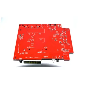
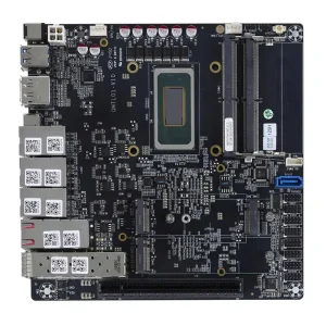
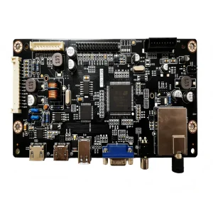
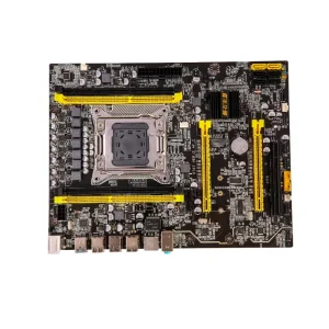
Explore our advanced PCBA capabilities serving high-reliability medical, automotive, industrial, and consumer markets.
Shenzhen STHL is a leading provider of high-quality electronics manufacturing services (EMS) based in China. We support international engineering and procurement teams along the entire product development lifecycle—ranging from PCB design layout optimization and full-scale global component sourcing to high-density PCB fabrication, precision SMT/THT PCBA assembly, complex cable assembly, mechanical box builds, and integrated structural functional testing.
Established in 2006, STHL has built over 20 years of experience in high-reliability electronics contract assembly. Our operations have expanded to support a growing customer base across the USA, Germany, Italy, UK, Poland, New Zealand, Brazil, Turkey, Korea, Thailand, and over 90 other regions worldwide.
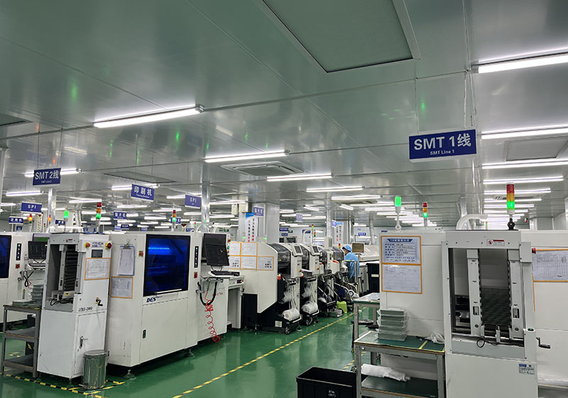
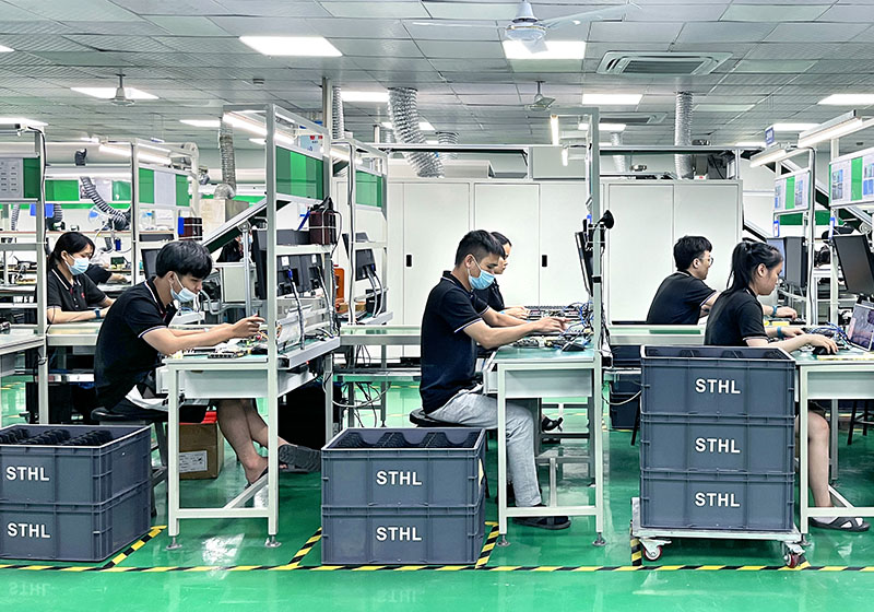
Operating out of a modern 10,000 sqm production facility staffed by 220+ highly skilled manufacturing personnel, STHL integrates advanced automation to deliver stability and repeatability. Our infrastructure features:
A granular look at the technical stages required to transform raw FR-4 and copper sheets into IPC Class 2 and Class 3 printed circuit boards.
Before fabrication, our engineers perform a rigorous Design for Manufacturability (DFM) check. We verify aspect ratios, drill-to-copper clearances, trace spacing, and thermal relief patterns to avoid production anomalies.
High-grade copper-clad laminates (FR-4, Rogers, High-Tg, or Polyimide for rigid-flex) are selected and cut to panel dimensions. Proper pre-baking is applied to remove residual moisture and ensure thermal stability during lamination.
The inner core panel is coated with a photosensitive dry film. Laser Direct Imaging (LDI) exposes the trace geometries. Developing baths remove unexposed film, leaving a precise resist pattern of the circuitry.
An acidic or alkaline etching process dissolves exposed copper, leaving protected traces. The remaining dry film resist is stripped chemically, revealing the exact inner layer copper layout.
Every inner layer is inspected using computerized AOI. High-definition cameras compare the physical traces against the original Gerber database, catching opens, shorts, and line-width variations before lamination.
Inner layer cores, resin-impregnated fiberglass (prepreg), and outer copper foil sheets are stacked under high temperature (up to 200°C) and pressure. This fuses the components into a rigid, monolithic multi-layer board.
High-speed mechanical CNC drills create through-holes for components and mounting. For blind and buried vias in high-density interconnect (HDI) designs, UV/CO2 laser drills are deployed to execute micro-via vias.
Through a chemical deposition process, a micro-thin layer of metallic copper is chemically coated onto the interior surfaces of the drilled holes. This sets up the electrical pathway between internal layers.
Liquid Photoimageable (LPI) Solder Mask is coated, exposed, and cured, leaving only the solder pads bare. The exposed copper is then plated with a surface finish (ENIG, HASL, OSP) to protect against oxidation.
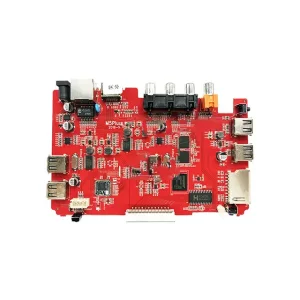
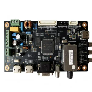
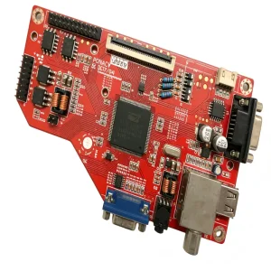
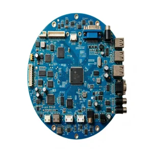
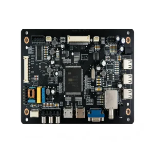
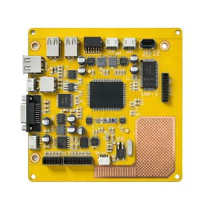
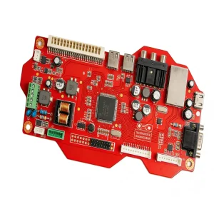
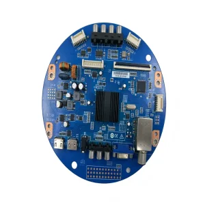
Combining automated surface mount technologies (SMT) and robust through-hole methods (THT) to handle advanced IC packages.
Our surface mount assembly lines handle fine-pitch packaging architectures. We routinely mount and solder complex componentry, including:
To guarantee long-term joint integrity, all SMT boards run through automated optical inspection (AOI) and 3D X-Ray laminography to catch hidden voids and bridge faults.
For assemblies subjected to mechanical shear, thermal shock, or high electrical current loads, THT remains a core requirement. Our line configurations encompass:
A single point of accountability from bare-board engineering to retail-ready box builds.
Operating 7 automated assembly lines configured for rapid prototyping and large-scale manufacturing runs. Fully certified for fine-pitch BGAs and multi-layer rigid-flex boards.
Production of high-reliability rigid, flexible, and rigid-flex multilayer substrates. We process high-Tg FR-4, Rogers, polyimide, and metal-core materials to spec.
Global supply network targeting original component manufacturers (OCMs). Real-time component tracking, alternative suggestions, and verification procedures protect your production schedule.
Precision wiring solutions incorporating custom overmolding, crimping, shielding jackets, and high-density connectors built to perform in rugged environment applications.
Complete mechanical system integration. We house the PCBA in metal or plastic enclosures, route internal cabling, mount displays, and package the product for final shipment.
Custom-built test benches verify hardware logic, analog inputs, and communication interfaces. Every board is flashed with firmware and thoroughly tested before shipment.
Mitigating components shortages and verifying quality through rigorous vendor audit protocols.
The global electronics component landscape is highly volatile. To secure component supply channels, STHL uses a multi-layered procurement model:
Our production floor operates under cleanroom-equivalent HVAC controls, implementing rigorous quality gates:
Adapting manufacturing lines to next-generation high-density, high-frequency, and eco-friendly electronics design.
As semiconductor geometries shrink, we are implementing any-layer HDI designs, utilizing stacked microvias filled with copper plating to maximize signal integrity while minimizing layer count.
Adopting specialized, low-loss dielectric materials (Rogers, PTFE, Megtron series) to handle high-frequency wireless communications, maintaining tight impedance tolerances down to +/- 5%.
Investing in halogen-free materials, energy-efficient reflow ovens, closed-loop water treatment systems, and recycling processes to minimize carbon footprint and chemical waste discharge.
Get direct, engineering-backed answers to standard PCB fabrication and assembly questions.
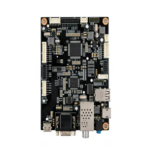
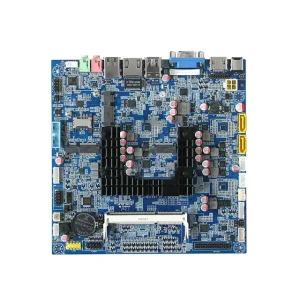
Explore our secondary product category highlighting complex industrial controllers, smart hardware, and imaging systems.