Explore our specialized production series engineered for critical-mission operations and regulatory compliance.
How cutting-edge technologies and modern compliance structures dictate the future of board components engineering.
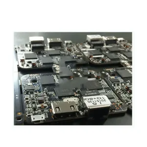
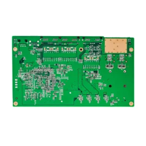
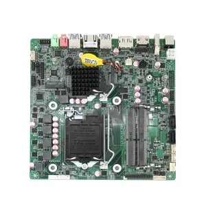
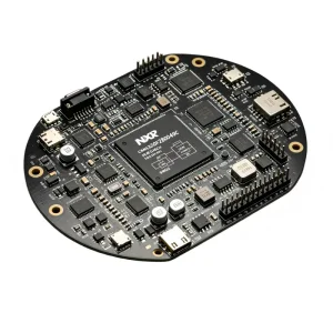
The global electronic components landscape is shifting rapidly towards high-density integration, thermal resilience, and AI-driven quality assurance. Across aerospace, medical devices, automotive propulsion, and industrial automation networks, PCBs are no longer passive substrates but complex operational elements. Modern printed circuit board assemblies must withstand harsher environments, consume less power, and transfer signals at higher frequencies than ever before.
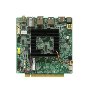
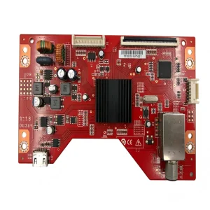
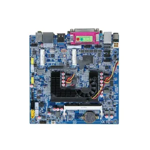
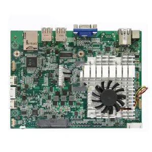
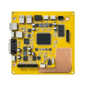
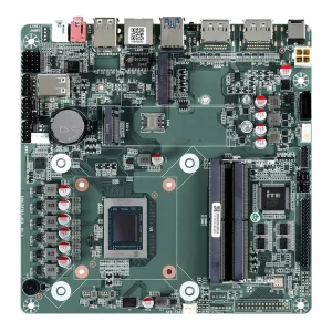
As an industry leader in Electronics Manufacturing Services (EMS), STHL coordinates a multi-tiered supply chain to mitigate raw materials risks while offering state-of-the-art SMT (Surface Mount Technology) and THT (Through-Hole Technology) pathways. From multi-layer HDI (High-Density Interconnect) fabrication to automated chemical passivation, we enable smart applications to transition from blueprint models directly to high-volume manufacturing.
Ensuring zero-defect manufacturing requires adhering to stringent international protocols. By integrating advanced testing metrics—such as automatic optical inspection (AOI), 3D X-ray microscopy, and specialized functional testbeds—we safeguard products intended for life-sustaining medical systems, ruggedized industrial terminals, and electric vehicle control modules.
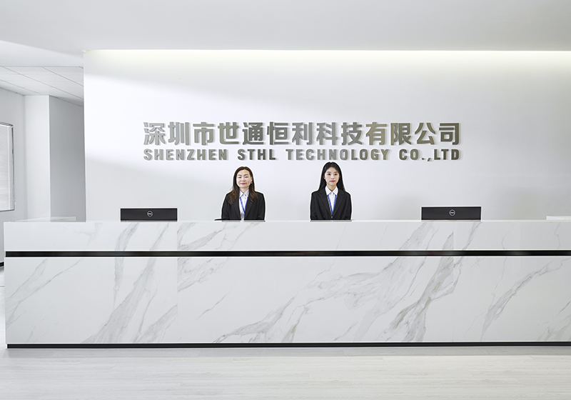
Established in 2006, Shenzhen STHL has developed into a premier partner for turnkey electronics contract assembly, boasting 20 years of experience in high-tier EMS. Based in the heart of China’s electronic innovation hub, our facility runs with 220+ highly skilled staff members managing 10,000 square meters of specialized workspace.
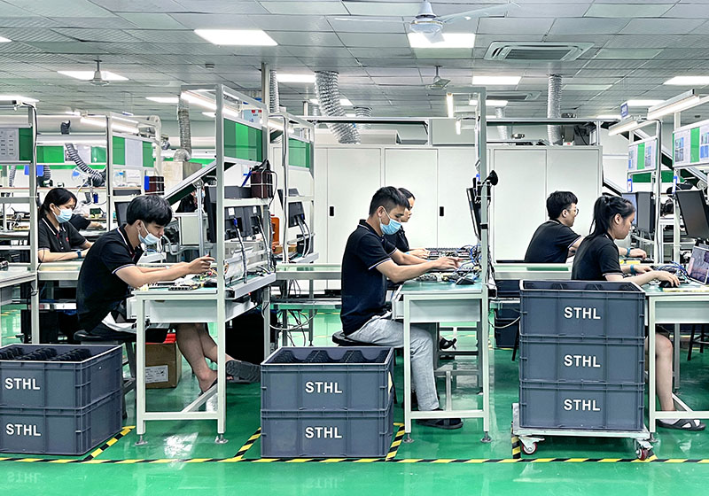
Our infrastructure contains 7 high-speed SMT assembly lines, 2 DIP/THT lines, 2 functional testing (FCT) lines, and 2 complete box-build assembly lines. We process products for diverse markets globally, including Energy Power, Telecommunications, Automotive, Medical, Consumer Electronics, and Smart IoT devices. We serve long-term clients across the USA, Germany, Italy, UK, Poland, Brazil, Korea, and 90 other regions worldwide.
Unlocking micro-pitch geometries and ultra-reliable solder connection technologies.
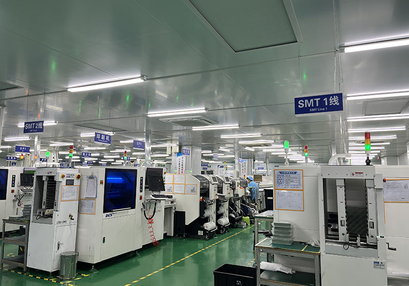
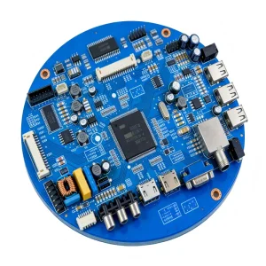
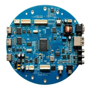
Surface Mount Technology is the core of modern electronic miniaturization. Our lines utilize pick-and-place equipment capable of placing micro-footprint parts at speeds designed for high-density boards.
We process complex packaging geometries including:
For high-stress environments where physical board endurance is paramount, Through-Hole components offer mechanical connections that surface mounting alone cannot match. Our manual and automatic DIP insertion lines maintain high durability standards.
From schematic review and multi-layer fabrication to global sourcing and turnkey box-builds.
Running 7 automated lines for prototype engineering and high-volume rollouts. Precise assembly, multi-zone reflow ovens, and lead-free alloy processing.
Delivering high-reliability HDI boards, flexible circuitry, and rigid-flex designs utilizing raw laminates for optimal thermal profiles.
Mitigate lead-time risks and protect against counterfeit components through global supplier networks. Real-time traceability for every BOM line item.
Full integration services including component fitting inside enclosures, complex wire harnesses, bezel placement, and final consumer packaging.
Rigorous test protocols including In-Circuit Testing (ICT), Boundary Scan, Temperature Chamber cycling, and customer-defined hardware emulation.
Custom cable assemblies including connectors, handles, internal retention shields, and shielding designs for heavy-duty industrial instrumentation.
Engineering complex circuit assemblies for demanding environments, from high altitudes to medical cleanrooms.
In fields like high-altitude tracking, data reference links (ADIRU), and aerospace instrumentation, component drift can disrupt operations. STHL uses temperature-stable dielectric layers and specialized high-reliability coatings to isolate circuits from moisture, altitude changes, and vibration.
Medical systems—such as infusion pumps, digital X-rays, ventilators, and biological monitors—require long-term operational stability. Following our ISO 13485 quality protocols, we use solder paste inspection (SPI) and X-ray analysis to verify joints and keep component quality consistent.
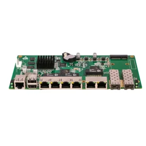
High-voltage distribution boards require careful spacing and clearance to prevent electrical arcing. We build heavy-copper PCBs that handle high power loads and deliver stable power conversion for solar systems, wind grid converters, and vehicle charging piles.
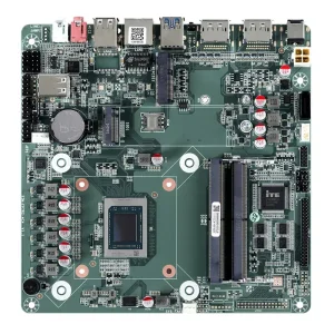
For smart display systems, tablets, and smartphone boards, we optimize multi-layer designs for heat dissipation. This helps devices maintain signal integrity and manage thermal loads during high-speed data processing.
Protecting your intellectual property, verifying material provenance, and maintaining export quality.
Operating on a global scale requires meeting stringent environmental and manufacturing standards. STHL complies with international directives like RoHS (Restriction of Hazardous Substances) and REACH, ensuring all component parts, solders, and coatings are free from hazardous chemicals. This supports clean recycling and aligns with environmental policies in North America and the European Union.
To prevent component issues, we use trace-level component validation protocols. Every reel of ICs, capacitors, or transistors is run through incoming quality inspection, verifying manufacturer batch codes against global distributor records. We also maintain secure data systems to protect clients' layout designs, firmware code, and project files.
Our team provides multi-language engineering support to assist with Design for Manufacturing (DFM) reviews. This helps resolve layout issues before fabrication starts, saving time and resources.
Adapting our manufacturing processes for the next generation of smart hardware designs.
As device sizes decrease, we are upgrading our pick-and-place lines to handle finer-pitch components and complex multi-layered substrate materials.
We are optimizing fabrication profiles for high-frequency applications, selecting low-loss dielectrics to maintain signal clarity at high frequencies.
We are integrating AI-driven optical and X-ray systems to detect micro-voids and potential assembly errors, ensuring high yield rates.
Technical and logisitical answers for sourcing managers, hardware designers, and operations leads.
Discover our advanced processing capabilities for heavy-power devices and consumer tech platforms.