High-performance custom electronic engineering and turnkey PCBA assemblies built to strict industrial, automotive, and medical tolerances.
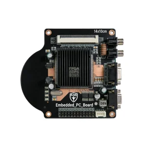
In modern electronics, the physical design layout of a Printed Circuit Board (PCB) acts as the fundamental bridge between theoretical circuit design and manufacturing yield. With components shrinking to sub-millimeter footprints and switching speeds scaling into gigahertz regimes, PCB layout is no longer just a task of routing traces—it is a critical exercise in high-frequency transmission line management, power integrity, and heat dissipation.
Global hardware vendors often face design challenges including parasitic inductance, electromagnetic interference (EMI), and thermal bottlenecks. Collaborating with an OEM manufacturer that provides in-house PCB layout services helps ensure that layouts are optimized for production. Designs are integrated with specific factory-floor parameters, including solder mask tolerances, pickup-nozzle constraints, thermal profiles of SMT reflow ovens, and localized component sourcing chains.
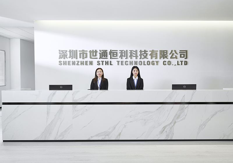
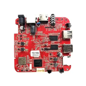
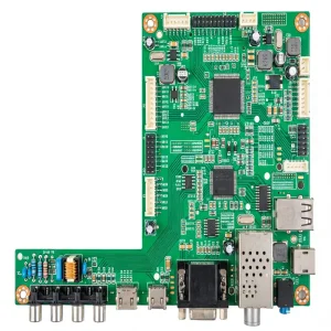
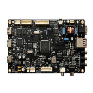
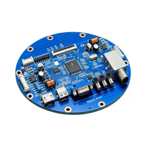
Established in 2006, Shenzhen STHL is an electronics manufacturing services (EMS) provider in China. We support international clients across the complete electronics product lifecycle, from initial PCB layout and schematic check to BOM component sourcing, PCB fabrication, SMT/THT assembly, custom cable routing, box build integration, and testing protocols.
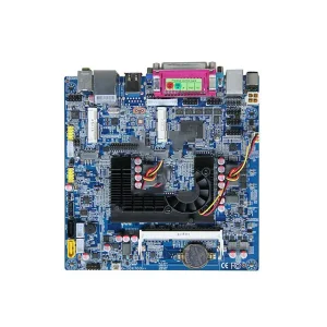
Operating from our 10,000 sqm production facility, we maintain modern equipment designed for quality and reliability. Our lines are calibrated to handle diverse configurations, including single-sided prototype cards and complex multilayer rigid-flex PCBs. We maintain compliance with standards such as RoHS, IATF16949, ISO9001, ISO14001, and ISO13485.
Supporting complex component packages with automated processing and comprehensive inspection methods.
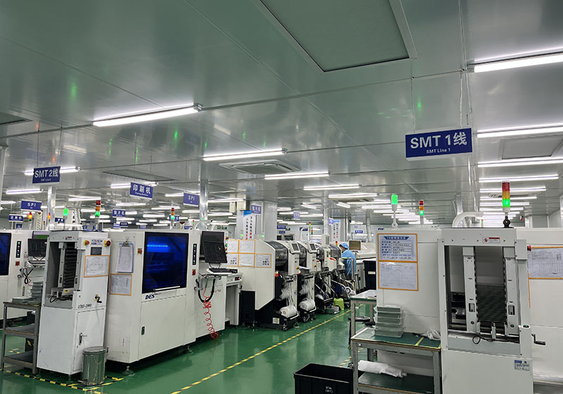
Our surface mount technology lines are configured for precision placement, handling fine-pitch components down to micro-BGAs and small passive chips (0201/01005 packages). Our processing capabilities include:
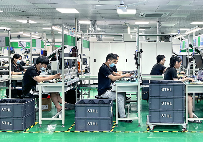
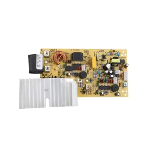
We support legacy designs and high-reliability industrial modules using manual and automated THT insertion, utilizing custom wave soldering fixtures to protect sensitive areas from heat damage.
Production processes are managed within static-safe (ESD) environments, using lead-free alloys to comply with environmental regulations such as RoHS and REACH.
Assembled boards undergo structural and electrical validation, using functional tests (FCT) and In-Circuit Testing (ICT) to check trace integrity and component alignment.
Complete turnkey support from raw component sourcing to boxed, tested, and retail-ready systems.
Operations feature 7 SMT lines configured to support prototype layouts and volume manufacturing, utilizing solder paste jetting and automated chip placement systems.
We manufacture rigid, flexible, and rigid-flex multilayered printed circuit boards using FR4, copper clad, and polyimide substrates to match electrical requirements.
We work with established distributors to procure genuine, traceable semiconductors and passives, assisting with lead time planning and obsolete part substitution.
We build custom interconnect systems, wiring looms, and heavy-gauge power lines using high-strength shielding to ensure signal integrity across chassis barriers.
We integrate completed PCB assemblies into metal, plastic, or custom molded enclosures, running cabling systems and testing operations in a single production loop.
We run custom FCT sequences on test benches to evaluate circuit pathways and electrical parameters, helping to minimize out-of-box failures.
For international system integrators, time-to-market is a critical metric. The concentration of component distributors, substrate manufacturers, and assembly plants in the Shenzhen electronics cluster helps streamline typical production timelines. Standard production stages that might require weeks in other markets—such as custom copper core fabrication, impedance verification, stencil adjustments, and parts sourcing—can often be completed locally in days.
Our proximity to local supply chains simplifies the process of finding alternatives for long-lead-time active components, such as microcontrollers and analog front-ends. This ecosystem supports quick prototyping, allowing designers to resolve issues before initiating mass production. This flexibility is particularly useful for complex projects like multi-gigabit network switch boards, high-current wind turbine regulators, and fine-pitch medical imaging electronics.
An effective PCB layout balancing performance and manufacturing cost requires early stage collaboration. Modern design methodologies prioritize Design for Manufacturing (DFM) and Design for Test (DFT) checks. Our team reviews layout files, schematic designs, and BOM structures to identify potential production issues early on. We analyze path routing, via placement, copper balance, and test point accessibility to verify they align with SMT machine specifications, helping to minimize delays during production ramp-up.
Providing specialized electronic assemblies tailored to the functional requirements of demanding operating environments.
We build wind turbine control boards and solar power systems designed to handle high voltages, thermal changes, and electrical noise. These designs feature thick copper cladding, isolation barriers, and thermal management via structural potting.
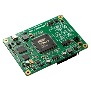
Our automotive body control modules (BCMs) and battery monitoring systems (BMS) are built on dedicated lines that meet IATF 16949 standards. They feature stable solder connections, vibration protection, and are designed to function reliably in under-the-hood environments.
We manufacture PCB assemblies for hearing aids, medical sensors, and CT scanners under ISO 13485 quality controls. These designs emphasize component traceability, high signal accuracy, and strict quality assurance.
As microprocessors become more complex, layout standards are moving toward High-Density Interconnect (HDI) structures with microvias, buried vias, and thin trace routing. Designers must manage high-speed signaling interfaces like PCIe Gen 5, DDR5, and USB4, which require careful trace alignment and impedance control to maintain signal clarity.
Additionally, modern systems generate more heat due to higher processing demands. Managing thermal transfer requires the use of metal core PCBs, heavy copper boards, and strategically placed thermal vias to dissipate heat from power components, protecting sensitive electronics in compact housings.
When selecting a contract manufacturer, global sourcing managers should verify key operational criteria, including:
Technical responses to common inquiries regarding layout guidelines, component sourcing, and assembly capabilities.
Before starting production, our engineering team performs a Design for Manufacturing (DFM) review. We check trace clearance, pad sizes, solder mask clearance, copper balance, and layer stack-ups against our production parameters. This step helps identify potential issues, such as solder bridging or tombstoning, before we build the physical boards.
We source components through authorized franchise distributors and verified partners. Our incoming quality control (IQC) team inspects shipment batches for correct manufacturer markings, barcode consistency, and package conditions, which helps prevent counterfeit parts from entering the assembly line.
Yes, we process multi-layer boards (up to 20 layers) using standard FR4, Rogers high-frequency laminates, polyimide flexible layers, and aluminum-clad thermal substrates. Our production processes are calibrated to handle hybrid materials that require precise temperature profiles during lamination.
We offer several testing and inspection methods, including 3D Automated Optical Inspection (AOI), In-Circuit Testing (ICT), functional testing (FCT) on custom test benches, and 3D X-Ray inspection for BGA packages to confirm solder joint alignment.
We maintain certifications that support high-reliability manufacturing, including IATF 16949 for automotive electronic modules and ISO 13485 for medical devices, alongside ISO 9001 and ISO 14001 quality management systems.
Our facility features assembly and testing areas for cable harnessing and box-build packaging. We manage the integration process, from installing finished PCBAs into metal or plastic enclosures to connecting internal cables and running functional system checks.
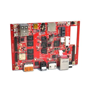
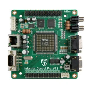
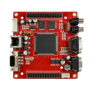
Providing custom circuit boards and complete assemblies for telecom, industrial lighting, and diagnostic instrumentation applications.