Explore our specialized PCB assembly and manufacturing capabilities serving major industries worldwide.
The global printed circuit board (PCB) and electronics manufacturing services (EMS) industries are undergoing a massive transition. As North American original equipment manufacturers (OEMs) demand high-reliability electronics, the concept of hybrid manufacturing ecosystems has emerged. While localized PCB fabrication services in the USA provide fast prototyping, NPI (New Product Introduction), and sensitive aerospace/defense processing under ITAR restrictions, scaling up to high-volume commercial production requires a seamless connection to highly mature global facilities. The integration of advanced manufacturing processes, rigorous quality standards, and diversified geographic supply chains is now the baseline for commercial success.
In high-tech sectors like automotive electrification, industrial IoT, medical diagnostic systems, and power grids, the demand for complex multilayer rigid, flex, and rigid-flex circuit boards is growing rapidly. USA-based system developers look for partners who can balance strict compliance controls with optimized cost structures. Leveraging automated PCB fabrication technologies alongside advanced SMT (Surface Mount Technology) assembly lines enables manufacturers to bridge the gap between design conceptualization and market-ready products. STHL, with its extensive track record of delivering end-to-end manufacturing solutions, stands as a premier supplier capable of meeting these precise engineering requirements.
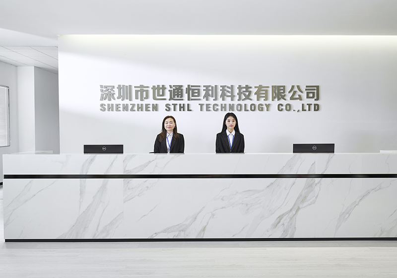
Shenzhen STHL is a high-quality provider of electronics manufacturing services (EMS) in China, serving customers worldwide along the whole industry chain including PCB layout, components sourcing, PCB fabrication, PCBA assembly, cable assembly, box build assembly and comprehensive testing services.
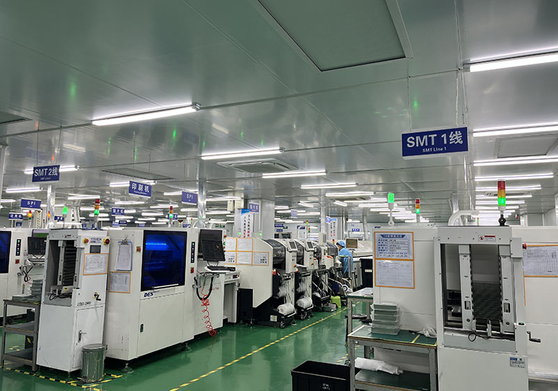
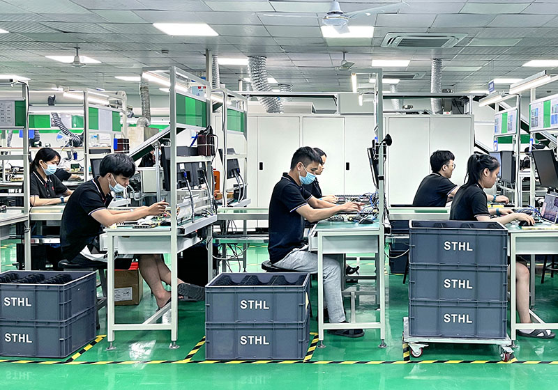
Established in 2006, STHL has built 20 years of experience in electronics contract assembly manufacturing. Our 10,000 sqm facilities are equipped with 7 automated SMT assembly lines, 2 DIP/THT lines, 2 functional testing lines, and 2 finished device assembly lines, supported by a dedicated team of over 220 professionals.
We provide high-precision electronics assembly for sectors including energy power, communications, automotive, medical, consumer electronics, computers & storage, safety & security, and industrial controls. Our customer base spans the USA, Germany, Italy, UK, Poland, New Zealand, Argentina, Brazil, Turkey, Korea, Thailand, and 90 other regions worldwide.
As an IATF16949, ISO9001, ISO14001, and ISO13485 certified manufacturer, we produce products that comply with RoHS standards and quality guarantees. Our advanced capabilities in materials analysis, reliability testing (AOI, X-RAY, ICT, and functional testing), and highly effective SMT/THT assembly make us a trusted partner for OEMs globally.
Handling ultra-fine pitch components requires precise thermal profiling and vision-guided placement machines. STHL specializes in mounting high-density, complex component arrays, ensuring structural integrity and electrical reliability under thermal and mechanical stress:
For high-power industrial control units, power distribution networks, and rugged applications, Through-Hole Technology (THT) remains essential for its high mechanical strength. STHL's THT processes include:
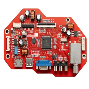
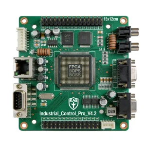
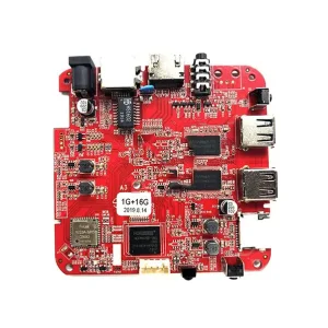
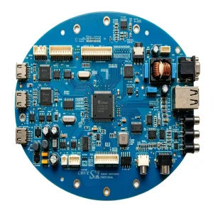
A complete suite of services from initial board fabrication through complex final product assembly.
We run 7 automated SMT lines for quick-turn prototyping and volume production. High-speed chip placers ensure precise alignment, while selective and wave soldering systems provide reliable THT connections.
Producing single-sided, multi-layer rigid, flex, and rigid-flex PCBs. We utilize high-Tg laminates, impedance control tracking, and precise laser drilling to meet demanding high-speed design guidelines.
Our supply chain network handles global procurement of certified electronic parts. We minimize counterfeit risks and allocation issues through end-to-end component traceability.
Custom cable assemblies and wire harnesses with integrated retention systems, shielding, and specialized connectors to withstand tough mechanical and environmental conditions.
Comprehensive electromechanical integration, including enclosure design fitting, sub-assembly routing, structural fastening, and complete system testing prior to product packaging.
Tailored testing solutions (FCT, ICT, boundary scan, thermal stress testing) to check functional operation under real-world simulations, preventing field failures.
Modern industrial systems demand high reliability and adherence to strict regulations. High-performance PCB fabrication and assembly are critical to the success of localized technology rollouts across North America:
The modernization of the electrical grid in the USA relies on high-power control systems. Wind turbine pitch controllers, commercial battery monitoring modules, and utility-scale power distribution units require thick copper layers (up to 4oz or more) to manage high currents. These systems demand robust thermal design, specialized isolation barriers, and compliance with UL standards to ensure continuous operation under extreme temperature variations.
Class II and Class III medical devices, such as ECG monitors, laboratory centrifuges, and diagnostic imaging equipment, demand strict adherence to quality management systems. Production runs are strictly governed by ISO13485 regulations. Traceability down to the raw material level, lead-free RoHS processing, and flawless SMT solder joins checked by automated X-ray analysis are required to guarantee patient safety and system reliability.
As electric vehicles (EVs) adopt higher battery voltages, vehicle battery packs and EV charging stations require advanced battery management systems (BMS). Printed circuit boards for these systems must handle high voltage, withstand mechanical vibration, and comply with the IATF16949 standard. To maintain functional safety in harsh environments, boards require high tracking resistance, selective conformal coating, and thermal interface materials.
Automated manufacturing environments rely on smart robotics that need compact, multi-layer control boards. By integrating high-density interconnect (HDI) designs with microvias and blind/buried structures, designers can pack processing power, sensor interfaces, and communications into very small footprints. These systems require precise impedance control and advanced shielding to prevent noise interference on the plant floor.
A forward-looking perspective on the technologies driving next-generation electronic hardware.
As system designs shrink, standard HDI approaches are shifting toward Substrate-Like PCBs (SLP). Using semi-additive fabrication methods (mSAP), manufacturers can achieve trace widths and spacings below 30/30 microns, allowing high-performance system-in-package solutions to be designed directly onto standard PCB substrates.
Deployments in 5G/6G communication systems require PCBs with low dielectric loss and high signal speeds. Standard FR-4 is increasingly replaced by Rogers, Teflon, and Megtron laminates. Incorporating metal cores and copper coins helps manage thermal challenges in high-frequency power amplifiers.
Embedding resistors, capacitors, and active silicon chips within the internal layers of multi-layer boards helps reduce external SMT footprints. This improves high-frequency performance by minimizing lead inductance and shielding internal circuits from external electromagnetic interference.
Integrating machine learning algorithms into 3D SPI (Solder Paste Inspection) and post-reflow AOI systems enables automated, real-time feedback loop adjustments. By analyzing defect trends in real time, placement parameters can be adjusted automatically, driving manufacturing defects down toward zero.
Get answers to critical engineering, manufacturing, and supply chain questions from our technical specialists.
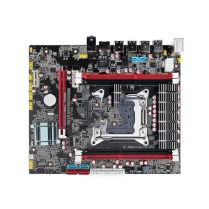
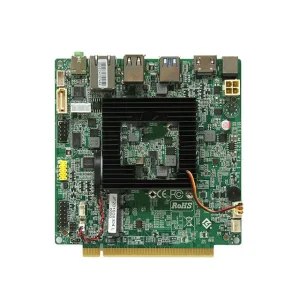
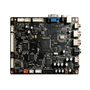
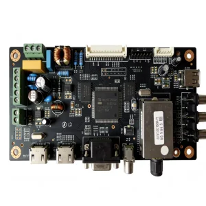
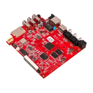
High-reliability circuit cards and electronic systems engineered for global performance requirements.