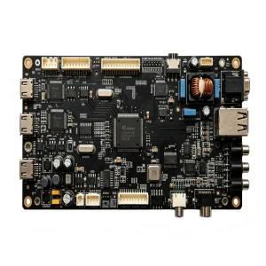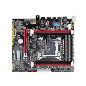
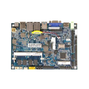
In the rapidly changing landscape of modern electronic engineering, the request for miniaturization, high-frequency signal processing, and heat dissipation efficiency has elevated the status of the Multi-Layer PCB from a mere interconnection component to a foundational subsystem. Historically, double-sided and simple multi-layer designs sufficed for conventional systems. Today's deep computing, Internet of Things (IoT), medical equipment, and automotive electrification industries demand boards ranging from 4 to over 32 layers, featuring High-Density Interconnect (HDI) structures, blind/buried vias, and advanced laminate materials.
As structural density increases, managing signal cross-talk, controlled impedance, and electromagnetic interference (EMI) becomes crucial. Global manufacturers are transitioning towards lower loss materials (such as PTFE and high-Tg FR4 blends) to combat the high-speed requirements of 5G, AI computing nodes, and advanced driver assistance systems (ADAS). As a veteran OEM Multi-Layer PCB manufacturer, STHL addresses these trends by refining the lamination process and optimizing layer stack-ups to guarantee impedance matching within ±5% to ±10% tolerances.
Shenzhen STHL is a premium provider of Electronics Manufacturing Services (EMS) based in China, catering to global clients across the entire value chain. We supply end-to-end support including PCB layout, component sourcing, PCB fabrication, PCBA assembly, cable assembly, box build assembly, and comprehensive functional testing.
Established in 2006, STHL has built 20 years of expertise in electronic contract manufacturing. Today, our team numbers over 220 professionals working inside a modern 10,000 sqm production facility. To meet strict demand timelines, our facility hosts 7 SMT assembly lines, 2 DIP/THT lines, 2 functional testing lines, and 2 complete box-build lines.
Operating under certifications like IATF 16949 (Automotive), ISO 9001 (Quality Management), ISO 14001 (Environmental Standards), and ISO 13485 (Medical Devices), we construct every electronic assembly in compliance with RoHS requirements. Advanced quality control methods, including AOI, 3D X-Ray inspection, and In-Circuit Testing (ICT), enable us to deliver reliable PCBA products to clients across Europe, the Americas, Asia, and Oceania.
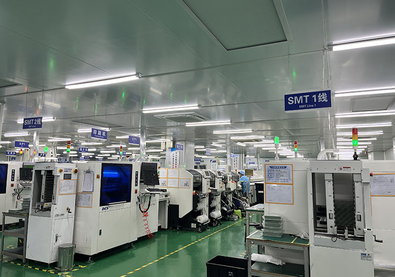
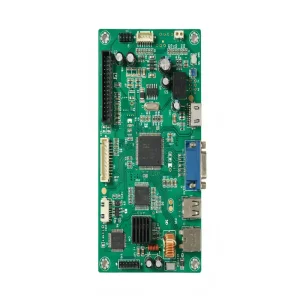
Handling high-density, multi-layer surface mount assemblies demands advanced placement machinery and clean environment controls. At STHL, our SMT processing setup is equipped to manage micro-miniaturized and ultra-fine-pitch component profiles, ensuring structural integrity and reliable solder joints.
Key SMT Assembly Capabilities Include:
Quality control validation integrates SPI (Solder Paste Inspection), online 3D AOI, and high-definition X-Ray systems to analyze joint integrity beneath BGA array packages.
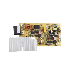
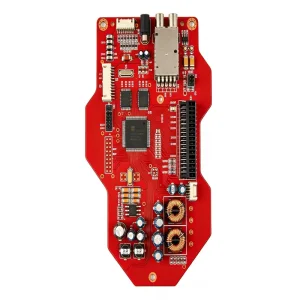
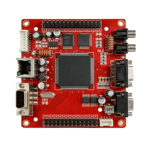
While surface-mount technologies handle high-density digital routing, Through-Hole Technology (THT) remains essential for heavy industrial electronics, high-power converters, automotive charging ports, and rugged medical units. Through-hole joints offer mechanical strength to survive thermal and mechanical stresses.
STHT THT Production Strengths:
Procuring multi-layer printed circuit board assemblies on a global scale presents supply chain challenges. Supply professionals must manage component allocation risks, track counterfeits, resolve lead time volatility, and ensure strict compliance with regional regulations (such as WEEE, REACH, RoHS, and CE guidelines).
STHL runs 7 automated lines for quick-turn prototyping and volume runs. Advanced placement equipment and selective wave soldering guarantee reliable joint assembly.
Fabricating high-layer-count rigid, flex, and rigid-flex boards. We use high-Tg laminates and handle controlled impedance and tight dielectric tolerances.
A global supply network verifies part origins and handles active component allocations. Traceability controls prevent counterfeit parts from entering assembly.
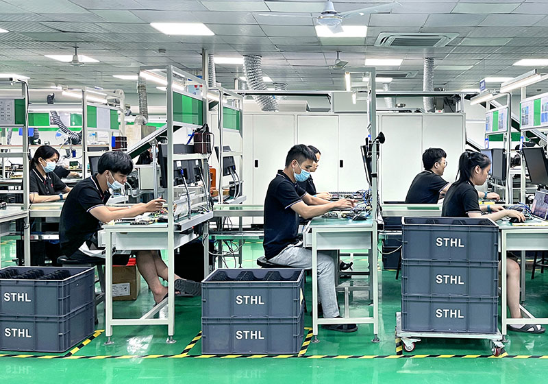
Full integration services, from PCBA enclosure installation to routing wire harnesses and packaging final products for direct distribution.
Precision custom shielding, connector termination, and strain reliefs, providing low-noise connections across demanding industrial environments.
Full-scale functional testing systems simulate operating parameters to confirm circuit stability and prevent field defects.
Working with an offshore manufacturer requires reliable communications and clear compliance verification. STHL maintains dedicated English-speaking project engineering teams to bridge time zone gaps. From DFM (Design for Manufacturability) analysis during layout validation to final delivery logistics, our staff supports clients across the US, Germany, Italy, UK, Poland, and 90 other regions.
Our plant aligns manufacturing workflows with international environmental and quality benchmarks:
Automotive quality standard compliance, ensuring safety and reliability across power components and engine ECUs.
Comprehensive medical device manufacturing standards, supporting infusion pump and air computer assemblies.
Robust internal process control frameworks combined with environmental footprint management policies.
As multi-layer PCB design trends toward complex integrations, STHL's engineering team is developing processes to support next-generation electronics architectures. Our technical development roadmap focuses on:
Expanding mass production capabilities to resolve trace-to-trace spacing below 3 mils, integrating fine-pitch BGA structures for AI edge computing and compact medical modules.
Standardizing hybrid stack-up layers combining low-loss Teflon (PTFE) laminates with traditional FR-4, reducing transmission losses in radar, RF, and high-frequency communication boards.
Embedding passives (resistors, capacitors) inside inner board layers to save exterior footprint area while improving overall heat dissipation profiles in high-power applications.