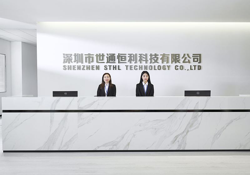
Shenzhen STHL is a premier, high-quality provider of Electronics Manufacturing Services (EMS) based in China, catering to a global customer base across the entire hardware lifecycle. Established in 2006, STHL has built 20 years of robust expertise in contract electronics assembly.
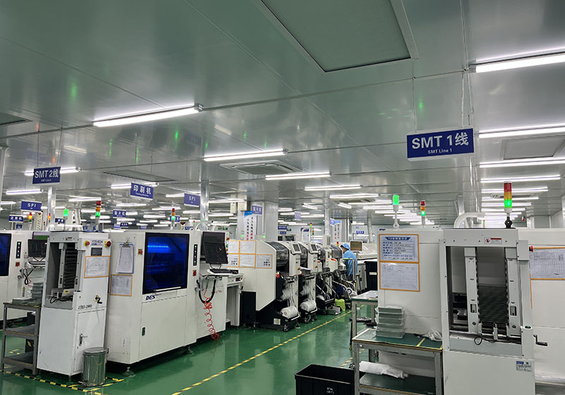
Operating from our advanced 10,000 square meter facility, we employ over 220 skilled specialists. Our state-of-the-art infrastructure houses 7 high-speed SMT assembly lines, 2 specialized DIP/THT lines, 2 dedicated functional testing lines, and 2 complete box-build integration lines. This dynamic setup allows us to seamlessly handle everything from prototyping to high-volume manufacturing runs.
By integrating strict quality systems such as IATF 16949 for automotive electronics, ISO 13485 for medical devices, ISO 9001, and ISO 14001, we ensure that every board shipped adheres to RoHS directives and IPC-A-610 Class II/III standards. We serve key markets worldwide, including the USA, Germany, Italy, the UK, Poland, New Zealand, Argentina, Brazil, Turkey, Korea, Thailand, and 90 other regions.
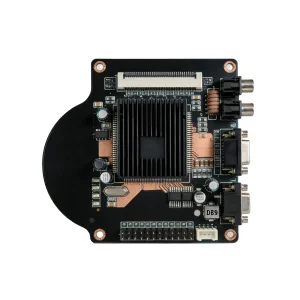
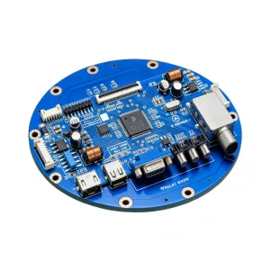
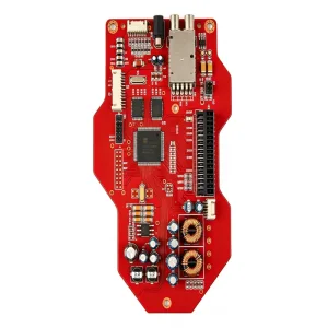
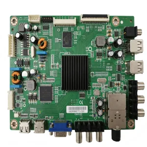
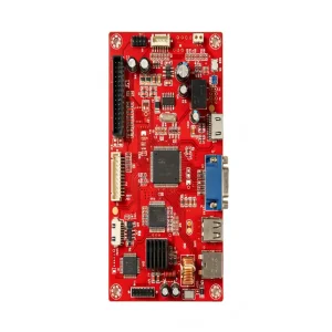
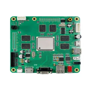
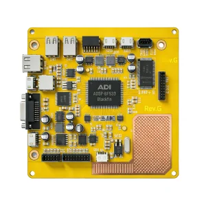
Modern electronic design demands extreme component density and microminiaturized footprints. STHL's engineering capability is specifically tuned to mount complex, fine-pitch active and passive components with repeatable accuracy.
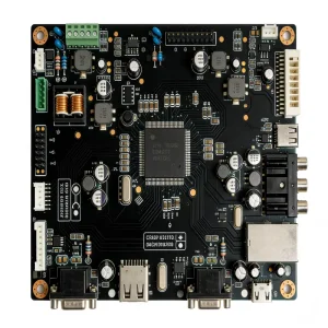
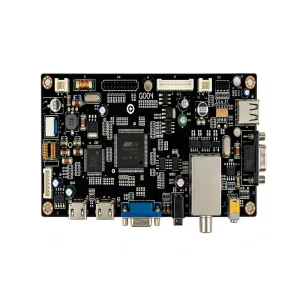
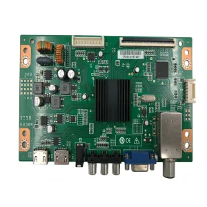
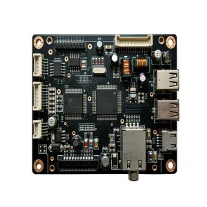
We possess extensive technical capability in mounting and inspection of:
Quality is guaranteed through automated Closed-Loop Solder Paste Inspection (SPI), high-resolution inline Automated Optical Inspection (AOI), and non-destructive 3D X-Ray Inspection for hidden solder joints on BGAs and leadless chips.
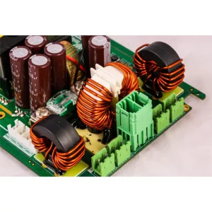
Despite the rapid migration to SMT, THT remains critical for power modules, connectors, and rugged industrial controllers that undergo significant mechanical stress and high electrical currents. STHL maintains a highly reliable THT infrastructure running in parallel with our SMT lines.
Our capabilities include:
7 highly automated SMT lines equipped with Yamaha and Samsung placement heads alongside dual wave-soldering DIP lines cover both fast-turn prototyping and high-volume multi-layer builds.
End-to-end bare board manufacturing. From simple double-sided PCBs to ultra-dense multi-layer structures, high-frequency RF materials, rigid-flex configurations, and metal cores.
Global supply chain partnerships with top-tier distributors. Mitigates counterfeit component entry, manages allocation risks, and secures hard-to-find components for production.
Precise processing of custom wire harnesses, mechanical shields, power lines, and terminal connectors to ensure signal integrity under extreme conditions.
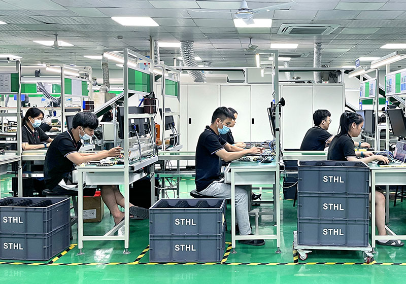
Turnkey system integration. We place the PCBA inside plastic or metal custom enclosures, wire sub-assemblies, run final functional tests, package and drop-ship to end consumers.
Complete testing regimes including ICT (In-Circuit Testing), custom dynamic FCT, environmental chamber thermal cycling, and boundary scan to deliver a 0% field failure rate.
Surface mount technology behaves differently under varying environmental parameters. A board designed for dry room testing may rapidly decay if deployed in high humidity agricultural fields or vibration-heavy engine compartments. By understanding these edge conditions, STHL optimizes layout and material sets for localization challenges.
Agricultural devices, such as soil detectors, are continuously exposed to soil acids, high moisture, and fluctuating temperatures. For localized stability, STHL implements selective Conformal Coating (acrylic, silicone, or polyurethane) to form a barrier against humidity and chemical contaminants. Solder alloys with low silver content or specialized micro-alloying additives are recommended to withstand low-frequency mechanical stress during probe insertion.
Water pollution monitoring stations and air scrubbers operate continuously in aggressive conditions. Thermal shocks can cause standard solder joints to micro-crack. STHL relies on localized CTE (Coefficient of Thermal Expansion) matching, specifying FR-4 substrates with high Tg (Glass Transition Temperature > 170°C) and custom multi-layer structures. This prevents delamination between copper layers and resin during high-heat cycles.
In miniature computing (such as tablet/smartphone PCBAs) and clinical automation setups, signal integrity is paramount. STHL implements microvia HDI (High-Density Interconnect) routing, stacked blind/buried vias, and zero-clearance component placing. Utilizing impedance-controlled stack-ups ensures zero noise crosstalk for gigahertz-speed signal runs.
Decoupling supply chains is complex because electronics manufacturing is highly dependent on sub-tier raw materials. Shenzhen represents a highly integrated industrial ecosystem, offering unmatched turnaround speed, component variety, and cost efficiency.
STHL operates within 2 hours of major raw material facilities, including copper clad laminates (CCL), specialty solder pastes, custom aluminum extrusions, and specialized tooling. This proximity reduces transit times and allows our team to address unexpected engineering design changes within hours rather than weeks.
When international markets experience semiconductor component shortages, STHL’s procurement team accesses verified domestic alternatives. This direct contact with original manufacturers avoids broker markups and ensures stable production lines during global components shortages.
As silicon dies shrink and electrical performance demands rise, conventional SMT approaches the limits of physics. STHL's technological roadmap aligns with upcoming market demands.
We are steadily transitioning our 7 SMT lines to use fully integrated, M2M (Machine-to-Machine) communication protocols. Feedback loops from the Solder Paste Inspection (SPI) system automatically calibrate the squeegee offset of the screen printers in real time. Similarly, post-reflow AOI systems feed deviation data back to pick-and-place systems to prevent placement drift before defects occur.
To minimize carbon footprints and support delicate substrates, STHL is testing bismuth-tin based LTS alloys. These allow peak reflow temperatures to drop from 250°C to below 190°C. This shift reduces thermal stress on integrated circuits, decreases PCB warpage, and lowers manufacturing energy usage by up to 25%.
Future electronic designs will embed passive components directly into the inner resin layers of the PCB substrate, freeing surface space for silicon. STHL's engineering team is working closely with raw PCB fabs to establish reliable laser-cavity milling and SMT mounting routines for buried passives, preparing for the next generation of high-frequency communications hardware.
Common technical issues resolved by our engineering division during Design for Manufacturing (DFM) reviews.