Direct integration of our high-quality contract manufacturing portfolio serving global critical industries.
Before exploring the manufacturing and supply chain nuances, engineers and sourcing teams must define the baseline structural and functional characteristics of both components.
In electronics manufacturing, the terms PCB (Printed Circuit Board) and PCBA (Printed Circuit Board Assembly) are frequently used interchangeably by non-specialists, yet they represent two completely distinct lifecycle phases of hardware development. Developing this clear separation is paramount when optimizing global supply chain configurations, estimating manufacturing costs, and defining quality control parameters.
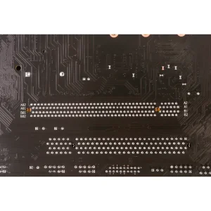
A bare PCB is a purely structural and passive electronic carrier containing non-conductive substrates (typically FR-4, Polyimide, or Ceramic) laminated with conductive copper pathways. It is completely inert and exhibits zero electrical functionality on its own.
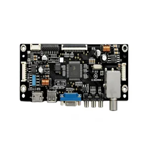
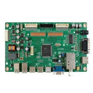
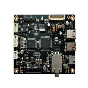
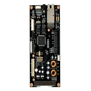
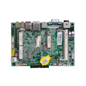
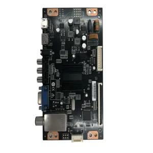
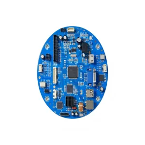
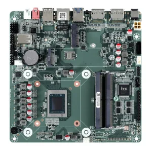
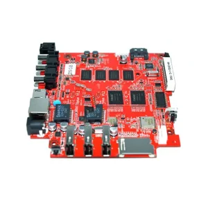
A PCBA, conversely, represents the completed, active subsystem. It is a PCB that has undergone component populating (soldering active components, passives, connectors, and integrated circuits via SMT or THT lines) and is fully prepared to execute processing instructions, power transmission, or signal translation.
| Comparison Vector | Bare PCB (Printed Circuit Board) | PCBA (Printed Circuit Board Assembly) |
|---|---|---|
| Functionality Status | Inert, structural carrier, non-functional component. | Fully functional, active thermodynamic & electrical subsystem. |
| Primary Components | Copper layers, substrate core, solder mask, silkscreen. | Bare PCB plus ICs, BGAs, capacitors, resistors, and connectors. |
| Manufacturing Processes | Chemical etching, drilling, copper plating, lamination. | Solder paste printing, Pick & Place (SMT), reflow, THT, inspection. |
| Quality Failure Modes | Delamination, open/short circuits, copper voids, misaligned vias. | Cold solder joints, tombstoning, voiding, component misalignment, ESD damage. |
| Testing Protocols | Flying probe test, Bed-of-Nails open/short electrical tests. | AOI (Automated Optical Inspection), X-Ray (3D AXI), ICT, Functional Testing (FCT). |
How macro-economic shifts, localized regulatory schemes, and geo-technological ecosystems define the global supply of bare boards and assembled systems.
While bare PCB fabrication is heavily consolidated in Asia (particularly mainland China, Taiwan, and Vietnam) due to high environmental processing requirements and chemical lamination infrastructure, PCBA services are becoming increasingly distributed. Regions like North America, Central Europe, and Southeast Asia are growing their localized PCBA capacities to support rapid prototyping, NPI (New Product Introduction), and aerospace or medical applications where physical proximity is crucial.
Modern OEMs (Original Equipment Manufacturers) are moving away from multi-vendor models where PCB fabrication and PCBA assembly are managed separately. Splitting the process creates supply chain vulnerability and leads to finger-pointing when failures arise. A unified contract manufacturer like STHL handles design validation, bare PCB fabrication, component sourcing, SMT/THT assembly, and functional testing under a single quality management system.
Industrial electronics must comply with strict regional standards like RoHS (Restriction of Hazardous Substances), REACH, and medical-grade ISO 13485 or automotive-grade IATF 16949. Standard bare PCB fabrication centers on chemical safety and mechanical safety, whereas PCBA factories focus heavily on trace level quality metrics like lead-free soldering verification, ESD (electrostatic discharge) safety zones, and real-time functional trace testing.
A direct look into high-precision assembly methodologies, equipment parameters, and quality testing paradigms.
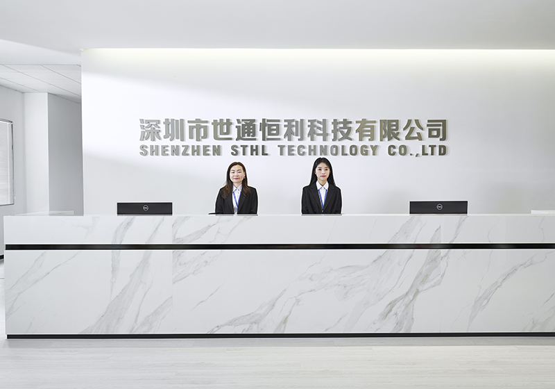
Shenzhen STHL is a premier high-quality provider of electronics manufacturing services (EMS) based in China, serving custom industrial portfolios worldwide. Our end-to-end operation covers the entire lifecycle of hardware production: starting with PCB layout verification, moving into components sourcing, PCB fabrication, PCBA assembly, cable assembly, box build assembly, and concluding with robust comprehensive testing services.
Established in 2006, our organization leverages 20 years of hardware contract assembly experience. Our ISO-certified 10,000 sqm production facility contains 7 high-speed SMT assembly lines, 2 specialized DIP/THT lines, 2 full-scale functional testing lines, and 2 complete box-build integration lines managed by a dedicated team of 220+ engineers and specialists.
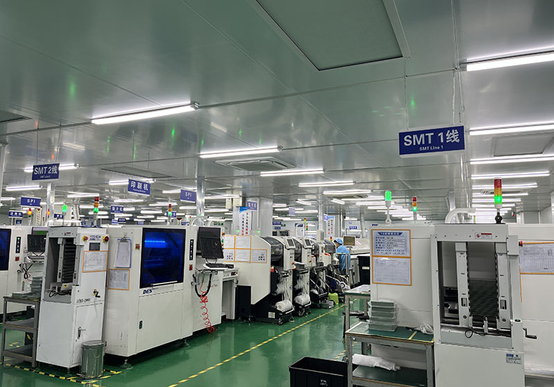
Surface Mount Technology (SMT) forms the backbone of modern high-density hardware manufacturing. STHL's automated SMT lines are configured to place complex, ultra-fine-pitch micro-electronics with micro-level repeatability.
To guarantee complete joint integrity on every SMT run, we utilize advanced inspection technologies. Every board is monitored using inline 3D Automated Optical Inspection (AOI) and high-performance 3D Transmission X-Ray Inspection (AXI) to identify internal solder voids or micro-bridges hidden beneath BGA packages.
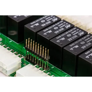
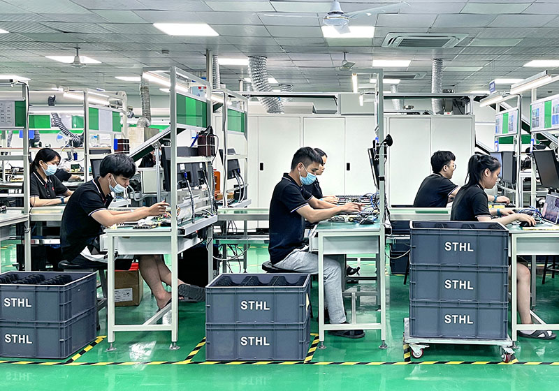
Despite the shift toward micro-SMT components, Through-Hole Technology (THT) remains essential for industrial systems requiring high mechanical durability, high-voltage operation, or thermal stress resistance.
As electronics become smaller, faster, and more heat-efficient, manufacturing techniques must evolve accordingly.
Future electronics demand higher component density within smaller areas. HDI technology uses microvias, stacked vias, and thin copper structures to route signals on multi-layered boards. Advanced PCBA lines must adapt to place components on trace pitches below 0.3mm with extreme accuracy.
Embedding passive resistors or capacitors directly into the internal layers of a bare PCB frees up valuable surface area. This approach reduces overall board size and improves signal integrity by shortening the distance between components, though it requires precise coordination between the board fabricator and the assembly line.
Artificial intelligence is reshaping inspection processes. AI models analyze 3D X-Ray and AOI scans to flag anomalies on assembly lines. This reduces false-calls, improves throughput, and prevents defects from passing through undetected.
The electronics industry is adopting greener materials, including halogen-free laminates, biodegradable substrates, and lead-free solder pastes. Optimizing reflow temperatures helps reduce the carbon footprint of factory operations without compromising mechanical reliability.
Different industries require unique engineering parameters. Here is how STHL tailors its PCB and PCBA capabilities to meet specific vertical challenges.
Compliance: ISO 13485, IPC Class 3.
Medical diagnostics and analytical instruments require reliable, long-term performance. We manage these requirements through strict trace-level component verification, component-level tracking, and robust functional testing to ensure complete diagnostic accuracy.
Compliance: IATF 16949, AEC-Q100 standards.
Automotive environments must withstand constant thermal cycling and mechanical vibration. We employ high-Tg materials, custom wave-solder fixtures, and dual-sided conformal coatings to protect assemblies from heat and vibration.
Compliance: UL 94V-0, IEC standards.
Power electronics deal with high voltages and currents. We build these systems using heavy copper PCBs, thick-film components, and automated wave-soldered connections to handle demanding power requirements safely.
STHL provides complete electronics manufacturing services, from initial board fabrication through to final box-build packaging.
STHL operates 7 automated PCB assembly lines for both prototype and mass production. Advanced SMT ensures precise component placement and quality. Skilled technicians provide efficient THT assembly and RoHS-compliant lead-free soldering.
STHL PCB fabrication service produces high-quality, reliable printed circuit boards from simple singles to complex multi-layers, from flex PCB to rigid-flexPCB, we use premium materials and controlled processes to meet precise specifications.
STHL offer global electronic component sourcing and supply chain solutions. Our vast supplier network and expertise ensure access to genuine, certified parts, mitigating risks of counterfeits, allocation, and long lead times to secure your production schedule.
With the precision manufacturing of cable assembly components including handles, retention systems, connectors, and shielding in a wide range of materials and finishes, we have performed many successful cable assembly for many customers from various industrial applications.
Making your projects at STHL from SMT assembly to box build assembly is very cost-effective and fast to market.Covering everything from putting a PCBAinto the enclosure with all functions testing to a complete product assembly packaged and ready for delivery to your customers,we can supply the full support.
STHL conducts functional testing (FCT) to verify product performance, preventing defects such as circuit issues, missing or incorrect components. This ensures delivered products are stable and fully qualified.
Answers to common technical, logistics, and engineering questions to help streamline your sourcing process.
PCB fabrication costs are determined by physical materials, laminate types (e.g., standard FR-4 vs. Rogers high-frequency material), layer counts, and mechanical processes like drilling and plating.
PCBA assembly costs, on the other hand, are driven by active component costs (ICs, microprocessors), assembly complexity (surface-mount vs. through-hole density), packaging types (such as fine-pitch BGAs), and the required testing protocols (like functional tests or 3D X-Ray inspection).
For bare PCBs, DFM focuses on structural board features, including copper trace widths, spacing, via sizes, and copper distribution across layers to prevent warping.
For PCBA, DFM looks at component placement, ensuring proper clearance for reflow nozzles, clear paths for wave soldering, appropriate pad sizes to prevent component tombstoning, and accessible test points for in-circuit testing (ICT).
Medical and automotive applications operate under strict safety standards. ISO 13485 requires detailed document control and clean assembly rooms to guarantee medical device sterility. IATF 16949 focuses on automotive reliability, requiring strict process controls and stress-testing protocols to ensure components can withstand continuous vibration and thermal cycling.
We work with authorized, direct distributors (like Arrow, Avnet, and DigiKey) and maintain a verified vendor rating system. Any component sourced from open markets undergoes verification, including visual checks, package-marking inspection, and electrical validation to prevent counterfeit parts from entering the assembly line.
Explore the rest of our specialty products, ranging from pulse oximeters to smart wear and energy solutions.