Explore our high-performance printed circuit board assemblies engineered for global industrial, medical, and consumer applications.
The backbone of modern electronics, offering the perfect balance between routing density, cost-efficiency, and mechanical reliability.
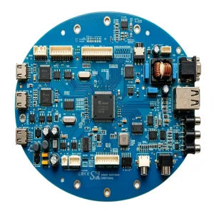
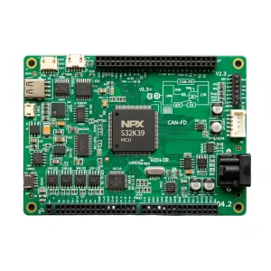
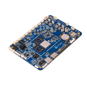
In the hierarchy of printed circuit board design, the Double-Sided PCB Board represents a critical technological milestone. Unlike single-sided boards, which restrict component placement and trace routing to a single conductive layer, double-sided boards utilize both the top and bottom layers. This is made possible through the implementation of Plated Through Holes (PTH), which serve as conductive pathways linking the circuit traces on either side of the substrate.
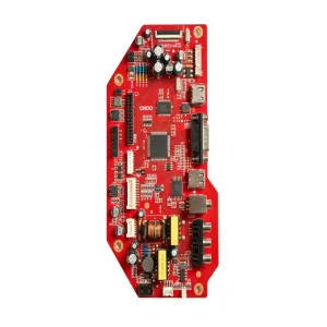
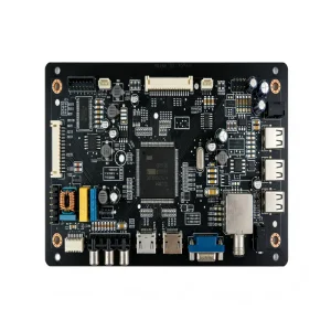
For global OEMs and system integrators, double-sided PCBs are the industry standard for applications requiring moderate circuit complexity. By allowing traces to cross over each other through vias, these boards dramatically increase routing density. This enables the integration of advanced surface-mount technology (SMT) and through-hole technology (THT) components on a compact footprint, making them indispensable for modern power supplies, industrial controls, and communication devices.
Shenzhen STHL is a premier, high-quality provider of electronics manufacturing services (EMS) based in China. We serve a diverse global clientele across the entire electronics lifecycle, offering integrated solutions that span PCB layout, components sourcing, PCB fabrication, PCBA assembly, cable assembly, box build assembly, and comprehensive functional testing services.
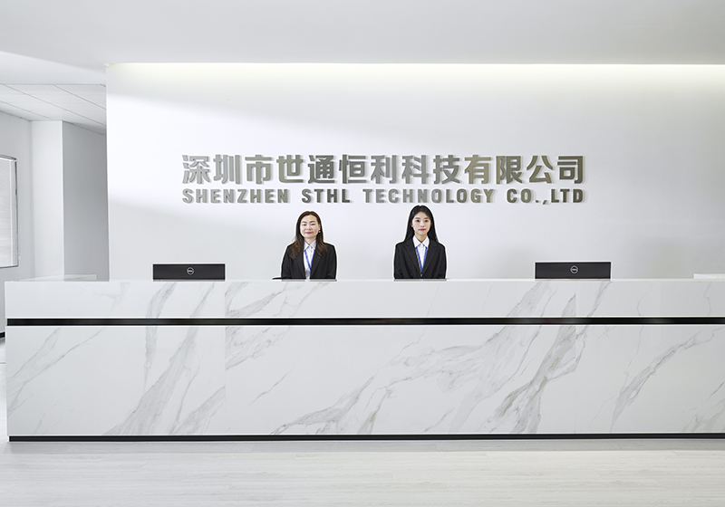
Established in 2006, STHL has built a formidable reputation over 20 years of experience in electronics contract assembly manufacturing. Today, our team of 220+ highly skilled professionals operates within a state-of-the-art 10,000 square meter facility. Our production infrastructure is designed for high-mix, variable-volume manufacturing, featuring:
As an IATF16949, ISO9001, ISO14001, and ISO13485 certified manufacturer, we adhere to the most stringent quality management systems. All products manufactured in our facility comply fully with RoHS and REACH standards, ensuring environmental safety and compliance for markets in the USA, Germany, Italy, UK, Poland, New Zealand, Brazil, Turkey, Korea, Thailand, and over 90 other countries.
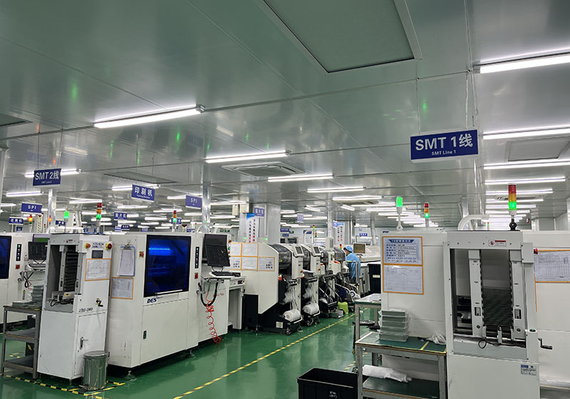
Surface Mount Technology (SMT) is the cornerstone of modern high-density electronics. At STHL, we leverage advanced automated placement systems to handle a wide range of complex, fine-pitch, and ultra-fine-pitch components with micron-level accuracy. Our technical capabilities include:
Our commitment to quality is backed by advanced inspection methodologies. Every SMT run undergoes automated optical inspection (AOI) and high-resolution 3D X-Ray inspection to detect hidden solder defects, bridging, or voids beneath BGA packages, guaranteeing flawless assembly before the boards proceed to functional testing.
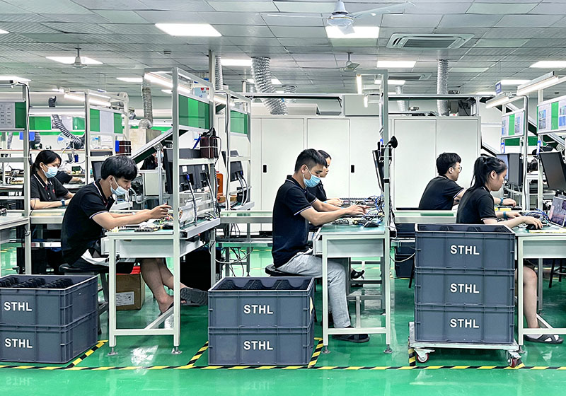
While SMT dominates high-density designs, Through-Hole Technology (THT) remains essential for components subjected to mechanical stress, high thermal loads, or high voltages—such as connectors, power transistors, and large electrolytic capacitors. STHL excels in THT assembly through a combination of manual precision and automated efficiency:
From initial design verification to final box-build packaging, we provide end-to-end electronics manufacturing services.
Operating 7 automated SMT lines and 2 DIP lines, we handle prototype runs and high-volume production with advanced reflow and wave soldering systems.
Manufacturing high-reliability double-sided and multilayer rigid, flexible, and rigid-flex PCBs using premium dielectric materials and copper weights.
An established global supply network ensuring access to genuine, traceable electronic components, mitigating counterfeit risks and supply chain delays.
Custom wire harness and cable assembly manufacturing, including shielding, overmolding, and heavy-duty connectors for industrial applications.
Full system integration, including PCB installation, enclosure assembly, internal cabling, software flashing, and final packaging for retail.
Rigorous FCT, ICT, boundary scan, and environmental stress screening to guarantee that 100% of shipped products perform to specification.
The strategic advantages of partnering with a Shenzhen-based EMS provider for global electronics manufacturing.
Shenzhen is the global epicenter of electronics manufacturing. Within a 50-mile radius, we have direct access to raw laminate manufacturers (FR4, Rogers, Megtron), component distributors, tooling shops, and surface treatment facilities. This close proximity reduces lead times for double-sided PCB fabrication and component sourcing from weeks to days.
Chinese PCB factories have transitioned from low-cost assembly shops to highly automated, smart manufacturing centers. At STHL, we utilize state-of-the-art SMT lines, automated optical inspection (AOI), 3D X-Ray, and selective wave soldering machines that match or exceed Western manufacturing standards at a fraction of the capital cost.
Whether you require a quick-turn prototype of 10 double-sided boards for design validation or a mass-production run of 100,000 units, our facility is structured to scale dynamically. We offer high-mix, low-volume flexibility alongside high-volume efficiency, allowing seamless transitions as your product matures.
Modern Chinese EMS providers prioritize international certifications. STHL operates under IATF16949 (automotive), ISO13485 (medical), and ISO9001 quality frameworks. Our adherence to IPC-A-610 Class 2 and Class 3 standards ensures that our double-sided PCBs meet the reliability requirements of critical industries.
Technological advancements shaping the future of double-sided printed circuit board design and manufacturing.
As consumer and industrial devices shrink, the demand for ultra-fine trace widths and spacings (down to 3 mils) on double-sided boards is rising. This requires advanced laser direct imaging (LDI) and vacuum etching processes to maintain signal integrity.
With the expansion of 5G, IoT, and high-speed radar, double-sided PCBs are increasingly utilizing high-frequency, low-loss laminates (such as Rogers or Teflon) instead of standard FR4 to minimize signal attenuation at gigahertz frequencies.
Environmental regulations are driving the adoption of halogen-free laminates, lead-free surface finishes (ENIG, OSP, Immersion Silver), and energy-efficient closed-loop water recycling systems in modern PCB fabrication factories.
How double-sided PCBs serve as the core engine for diverse industrial sectors globally.
In the automotive sector, double-sided PCBs are widely used in Battery Management Systems (BMS), LED lighting modules, and climate control units. These boards must withstand extreme thermal cycling and mechanical vibration. STHL's IATF16949 certification guarantees that our manufacturing processes meet the zero-defect requirements of automotive OEMs.
From anesthesia machines to MRI imaging workstations, medical electronics demand absolute reliability. Double-sided PCBs in these devices require high-grade FR4 substrates (TG170 or TG180) and precise impedance control. Our ISO13485 certification ensures complete component traceability and rigorous functional testing for medical-grade assemblies.
Industrial PLC controllers, power quality analyzers, and motor drives rely on heavy copper double-sided PCBs to handle high currents and manage thermal dissipation. We offer customized PCB fabrication with copper thicknesses up to 4oz, combined with selective wave soldering for heavy-duty THT terminals.
Smart thermostats, voice assistants, and home hubs require compact, cost-effective double-sided PCBs integrated with RF modules (Wi-Fi, Bluetooth, Zigbee). STHL provides turnkey PCBA services, including RF shield installation, antenna tuning verification, and complete plastic enclosure box-build assembly.
Mitigating risks, ensuring component authenticity, and optimizing logistics for international buyers.
For procurement managers in the USA, Europe, and Asia, sourcing PCBs internationally involves managing risks related to lead times, component obsolescence, and quality consistency. STHL addresses these challenges through a robust supply chain management framework:
Answers to the most common engineering and procurement questions regarding double-sided PCB fabrication and assembly.
For standard double-sided PCBs, we can reliably manufacture trace widths and spacings down to 3 mils (0.075mm) for prototype runs and 4 mils (0.1mm) for mass production. This allows for high-density routing around fine-pitch components like 0.4mm pitch BGAs.
We utilize high-precision solder paste printers with SPI (Solder Paste Inspection) to ensure uniform paste volume. Our reflow ovens feature multi-zone temperature profiling tailored to the specific thermal mass of the board. Post-reflow, we perform 100% 3D X-Ray inspection (AXI) to detect and quantify any voiding, bridging, or open joints beneath leadless packages.
We offer HASL (Lead-Free), ENIG (Electroless Nickel Immersion Gold), OSP (Organic Solderability Preservatives), and Immersion Silver. For fine-pitch SMT components and long shelf life, ENIG is highly recommended due to its flat surface and excellent oxidation resistance. For cost-sensitive consumer applications with standard pitch components, HASL or OSP is often preferred.
Yes, STHL is fully committed to environmental sustainability. We offer completely lead-free manufacturing processes, utilizing RoHS-compliant laminates, solder pastes, and surface finishes. We provide full material declaration sheets upon request to support your compliance audits.
Absolutely. Our turnkey services extend beyond PCB assembly. We have 2 dedicated finished device assembly lines where we install PCBAs into custom plastic or metal enclosures, integrate wire harnesses, perform firmware flashing, and conduct comprehensive functional testing (FCT) to ensure the product is retail-ready.
Discover more specialized electronics manufacturing capabilities designed to meet your specific industry standards.